CY7C68013
Document #: 38-08012 Rev. *A Page 5 of 48
1.0 EZ-USB
®
FX2
™
Features
Cypress’s EZ-USB
®
FX2
™
is the world’s first USB 2.0 integrated microcontroller. By integrating the USB 2.0 transceiver, SIE,
enhanced 8051 microcontroller, and a programmable peripheral interface in a single chip, Cypress has created a very cost-
effective solution that provides superior time-to-market advantages. The ingenious architecture of FX2 results in data transfer
rates of 56 Mbytes per second, the maximum allowable USB 2.0 bandwidth, while still using a low-cost 8051 microcontroller in
a package as small as a 56 SSOP. Because it incorporates the USB 2.0 transceiver, the FX2 is more economical, providing a
smaller footprint solution than USB 2.0 SIE or external transceiver implementations. With EZ-USB FX2, the Cypress Smart SIE
handles most of the USB 1.1 and 2.0 protocol in hardware, freeing the embedded microcontroller for application-specific functions
and decreasing development time to ensure USB compatibility. The General Programmable Interface (GPIF) and Master/Slave
Endpoint FIFO (8- or 16-bit data bus) provides an easy and glueless interface to popular interfaces such as ATA, UTOPIA, EPP,
PCMCIA, and most DSP/processors.
Three packages are defined for the family: 56 SSOP, 100 TQFP, and 128 TQFP.
• Single-chip integrated USB 2.0 Transceiver, Serial Interface Engine (SIE), and Enhanced 8051 Microprocessor
• Software: 8051 runs from internal RAM, which is:
— Downloaded via USB, or
— Loaded from EEPROM
— External memory device (128-pin configuration only)
• Four programmable BULK/INTERRUPT/ISOCHRONOUS endpoints
— Buffering options: double, triple and quad
• 8- or 16-bit external data interface
• General Programmable Interface (GPIF)
— Allows direct connection to most parallel interfaces; 8- and 16-bit
— Programmable waveform descriptors and configuration registers to define waveforms
— Supports multiple Ready (RDY) inputs and Control (CTL) outputs
• Integrated, industry standard 8051 with enhanced features:
— Up to 48-MHz clock rate
— Four clocks per instruction cycle
— Two USARTS
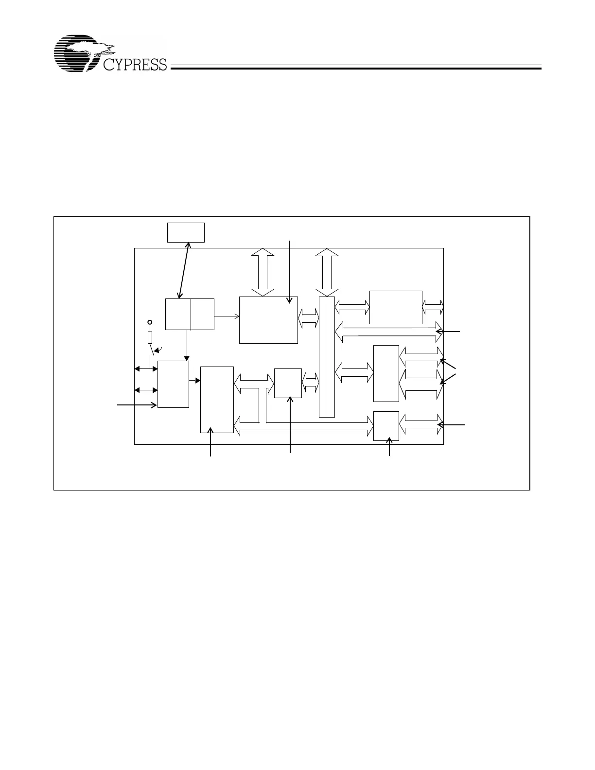
Address (16)
x20
PLL
/0.5
/1.0
/2.0
8051 Core
12/24/48 MHz,
four clocks/cycle
I
2
C
Compatible
V
CC
1.5k
D+
D–
Address (16) / Data Bus (8)
FX2
GPIF
CY
Smart
USB
1.1/2.0
Engine
USB
2.0
XCVR
8.5 kB
RAM
4 kB
FIFO
Integrated
full- and high-speed
XCVR
Additional I/Os (24)
ADDR (9)
CTL (6)
RDY (6)
8/16
Data (8)
24 MHz
Ext. XTAL
Enhanced USB core
Simplifies 8051 core
“Soft Configuration”
Easy firmware changes
FIFO and endpoint memory
(master or slave operation)
Up to 96 MBytes/s
burst rate
General
programmable I/F
to ASIC/DSP or bus
standards such as
ATAPI, EPP, etc.
Abundant I/O
including two USARTS
High-performance micro
using standard tools
with lower-power options
Master
Figure 1-1. Block Diagram
connected for
full speed