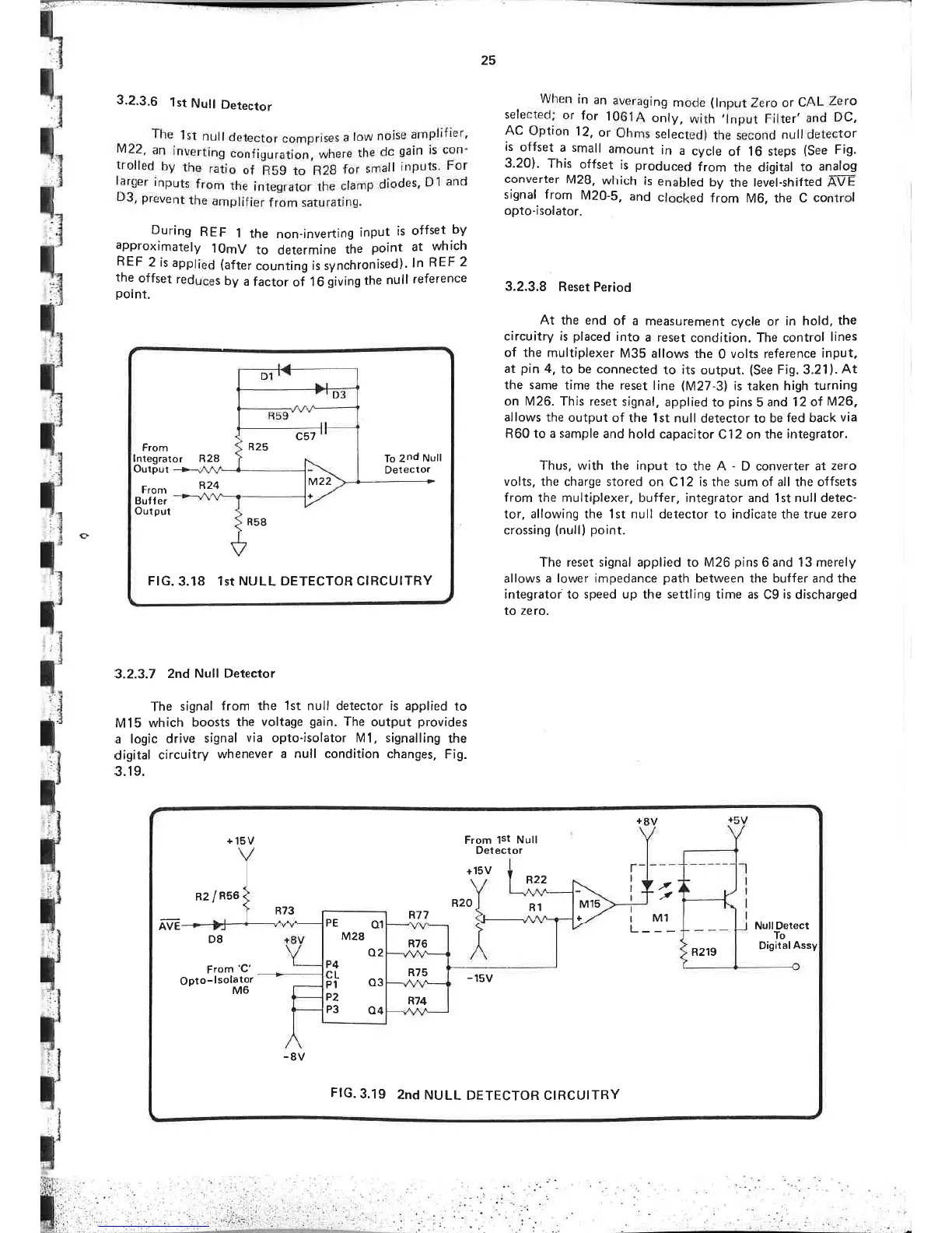
3.2.3.6
lst
Null
Detector
lst
null
detector
comprises
a
low
noise
amplifier,
M22,
an
inverting
configuration,
where
the
dc
gain
is
con-
trolled
by
the
ratio
of
RSg to R28
for
small
inputs'
For
larger
inputs
from
the
integrator
the
clamp
diodes,
D1
and
D3, prevent
the
amplifier
from
saturating.
When
in
an
averaging
mode
(lnput
Zero
or
CALZero
selected;
or
for
10614
only,
with
,lnput
Filter,
and
DC,
AC
Option
12,
or
Ohms
selected)
the
second
null
detector
is
offset
a
small
amount
in
a cycle
of
16 steps
(See
Fig.
3.20).
This
offset
is
produced
from
the digital
to
analog
converter
M28,
which
is
enabled
by
the level-shifted
ÃVE
signal from
M20-5,
and
clocked
from
M6, the
C
control
opto-isolator.
3.2.3.8
Reset
Period
At the
end
of a
measurement
cycle or
in hold,
the
circuitry is
placed
into
a reset
condition. The control
lines
of
the
multiplexer
M35
allows
the 0
volts reference
input,
at
pin
4,
to be connected
to
its
output.
(See
Fig.3.21).
At
the same
time the reset
line
(M27-3)
is
taken
high turning
on M26. This reset
signal,
applied
to
pins
5
and 12 of
M26,
allows the
output
of the 1st
null detector to be
fed back
via
R60
to a sample
and
hold capacitor
C12 on
the integrator.
Thus, with
the
input
to
the A
-
D converter at
zero
volts, the charge stored
on C12
is
the sum
of
all the offsets
from
the multiplexer, buffer, integrator
and
1st null detec-
tor, allowing the 1st null detector
to
indicate
the true
zero
crossing
(null)
point.
The
reset signal applied to M26
pins
6 and l3 merely
allows
a lower impedance
path
between the buffer and the
integrator to speed up the settling time as
C9
is
discharged
to
zero.
25
o
During
REF
1
the
non-inverting
input
is
offset
by
approximately
1OmV
to
determine
the
point
at
which
REF
2 is
applied
(after
counting
is
synchronised).
ln
REF
2
the
offset
reduces
by
a
factor
oi
t
6
giuing the
null
reference
point.
M22
+
c57
R25
From
lntegra
Output
tor
R28
To znd
Null
Detec
tor
Fronr
Bul fer
Out
put
R24
R58
F|G.3.18
lst
NULL DETECTOR CIRCUITRY
3.2.3.7
2nd
Null Detector
The
signal
from
the
lst null detector is
applied to
M15
which
boosts
the
voltage
gain.
The
output
provides
a logic
drive
signal
via
opto-isolator
M1,
signalling
the
dígital
circuitry
whenever
a
null condition
changes,
Fig.
3.1
9.
M15
+
R76
R75
R74
M28
P4
CL
P1
P2
P3
PE
o1
o2
o3
o4
R219
Null Detect
To
Diqiral
Assy
,
.t
-15V
-8V
+
15V
R2
lR56
+
+
R77
R73
AVE
R1
D8
Í
I
I
I
F!G.3.19
Znd
NULL
DETECTOR CIRCUITRY
R22
R20
+15V
rMl
L___
FfOm
U
ODto-
lsolator
'M6
From 1st
Null
Detector