15
AVR-2801/981
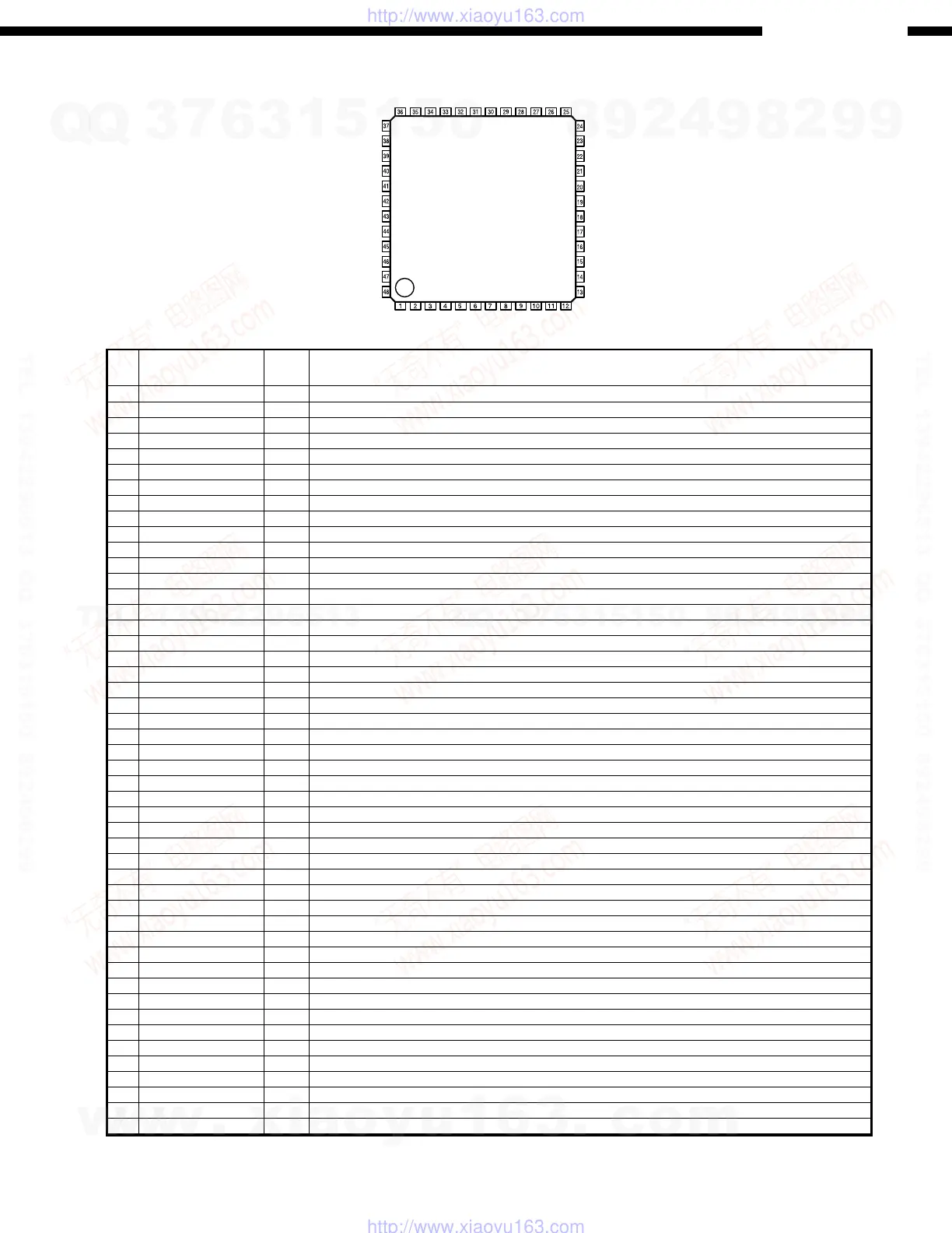
LC89055W (AU: IC800)
Pin Name
Function
LC89055W Terminal Function
Pin
No.
1 DISEL I Data input terminal (select input pin of DIN0, DIN1)
2 DOUT O Input bi-phase data through output terminal
3 DIN0 I Amp built-in coaxial/optical input correspond data input terminal
4 DIN1 I Amp built-in coaxial/optical input correspond data input terminal
5 DIN2 I Optical input correspond data input terminal
6 DGND Digital GND
7 DVDD Digital power supply
8 R I VCO gain control input terminal
9 VIN I VCO free-run frequency setting input terminal
10 LPF O PLL loop filter setting terminal
11 AVDD Analog power supply
12 AGND Analog GND
13 CKOUT O Clock output terminal (256fs, 384fs, 512fs, X′tal osc., VCO free-run osc.)
14 BCK O 64fs clock output terminal
15 LRCK O fs clock output terminal (L: Rch, H: Lch, I2S: Reverse)
16 DATAO O Data output terminal
17 XSTATE O Input data detecting result output terminal
18 DGND Digital GND
19 DVDD Digital power supply
20 XMCK O X′tal osc. clock output terminal (24.576MHz or 12.288MHz)
21 XOUT O X′tal osc. connection output terminal
22 XIN I X′tal osc. connection output terminal
23 EMPHA O Emphasis information output terminal of channel status
24 AUDIO O Bit1 output terminal of channel status
25 CSFLAG O Top 40bit revise flag output terminal of channel status
26 F0/P0/C0 O Input fs cal. sig. out / data type out / input word inf. output terminal
27 F1/P1/C1 O Input fs cal. sig. out / data type out / input word inf. output terminal
28 F2/P2/C2 O Input fs cal. sig. out / data type out / input word inf. output terminal
29 VF/P3/C3 O Validity flag out / data type out / input word inf. output terminal
30 DVDD Digital power supply
31 DGND Digital GND
32 AUTO O Non PCM burst data transfer detect sig. output terminal
33 BPSYNC O Non PCM burst data preamble Pa, Pb, Pc, Pd sync sig. output terminal
34 ERROR O PLL lock error, data error flag output terminal
35 DO O CPU I/F read data output terminal
36 DI I CPU I/F write data input terminal
37 CE I CPU I/F chip enable input terminal
38 CL I CPU I/F clock input terminal
39 XSEL I Frequency select input pin of XIN X′tal osc. (24.576MHz or 12.288MHz)
40 MODE0 I Mode setting input terminal
41 MODE1 I Mode setting input terminal
42 DGND Digital GND
43 DVDD Digital power supply
44 DOSEL0 I Data output format select input terminal
45 DOSEL1 I Data output format select input terminal
46 CKSEL0 I Output clock select input terminal
47 CKSEL1 I Output clock select input terminal
48 XMODE I Reset input terminal
I/O
* For latch-up countermeasure, set digital (DVDD) and analog (AVDD) power on/off in the same timing.
DISEL
DOUT
DIN0
DIN1
DIN2
DGND
DVDD
R
VIN
LPF
AVDD
AGND
AUDIO
EMPHA
XIN
XOUT
XMCK
DVDD
DGND
XSTATE
DATA0
LRCK
BCK
CKOUT
CE
CL
XSEL
MODE0
MODE1
DGND
DVDD
DOSEL0
DOSEL1
CKSEL0
CKSEL1
XMODE
DI
DO
ERROR
BPSYNC
AUTO
DGND
DVDD
VF/P3/C3
F2/P2/C2
F1/P1/C1
F0/P0/C0
CSFLAG
w
w
w
.
x
i
a
o
y
u
1
6
3
.
c
o
m
Q
Q
3
7
6
3
1
5
1
5
0
9
9
2
8
9
4
2
9
8
T
E
L
1
3
9
4
2
2
9
6
5
1
3
9
9
2
8
9
4
2
9
8
0
5
1
5
1
3
6
7
3
Q
Q
TEL 13942296513 QQ 376315150 892498299
TEL 13942296513 QQ 376315150 892498299
http://www.xiaoyu163.com
http://www.xiaoyu163.com
 Loading...