MX25L6406EM2I-12G (DIGITAL_DSP : IC782)
Block diagram
7
P/N: PM1548
REV. 1.2, JUL. 02, 2010
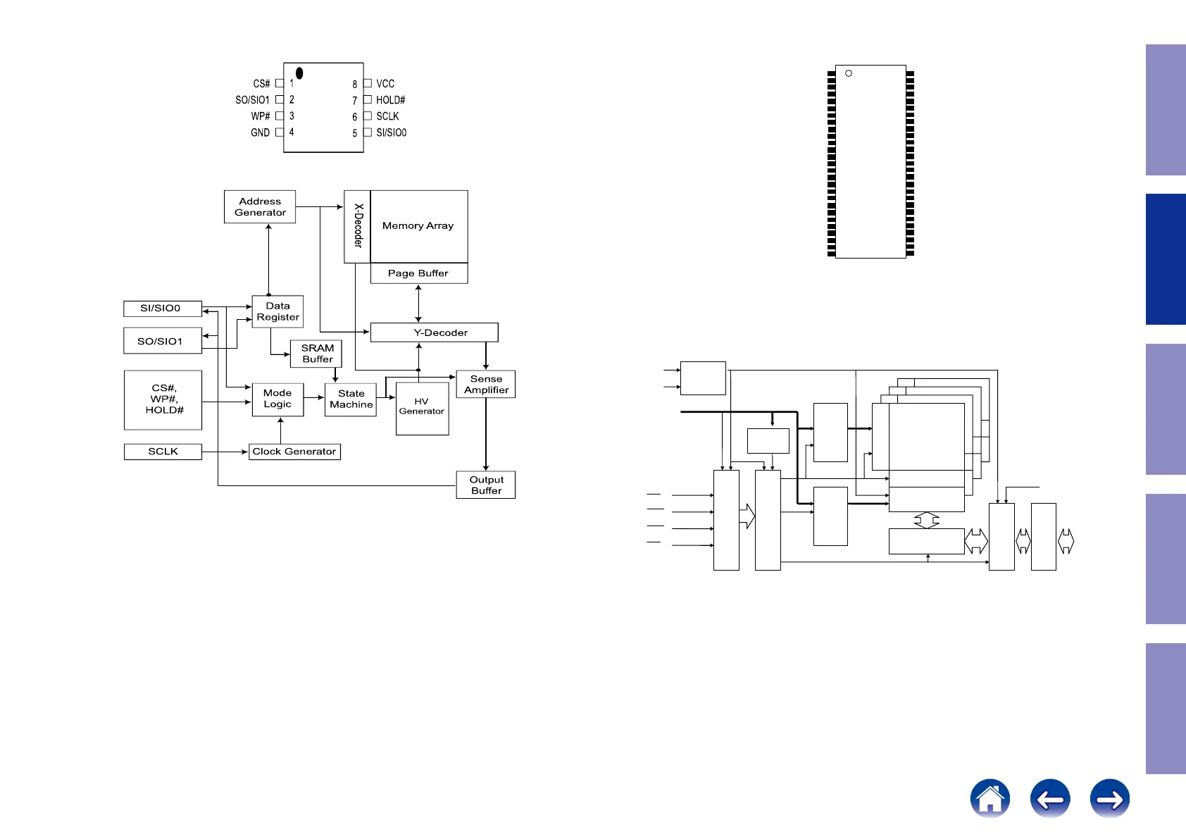
PIN CONFIGURATIONS
SYMBOL DESCRIPTION
CS# Chip Select
SI/SIO0
Serial Data Input (for 1 x I/O)/ Serial Data
Input & Output (for Dual Output mode)
SO/SIO1
Serial Data Output (for 1 x I/O)/ Serial Data
Output (for Dual Output mode)
Clock Input
WP# Write protection
HOLD#
Hold, to pause the device without
deselecting the device
VCC
GND Ground
PIN DESCRIPTION
16-PIN SOP (300mil) for MX25L1606E only
8-LAND WSON (6x5mm), USON (4x4mm)
8-PIN SOP (200mil, 150mil)
8-PIN PDIP (300mil)
8
P/N: PM1548
REV. 1.2, JUL. 02, 2010
BLOCK DIAGRAM
M12L64164A-5TG2Y (DIGITAL_DSP : IC784)
Block diagram
A3V64S40GTP
64M Single Data Rate Synchronous DRAM
Revision 1.0 Dec., 2012
CLK : Master Clock U,LDQM : Output Disable / Write Mask
CKE : Clock Enable A0-11 : Address Input
/CS : Chip Select BA0,1 : Bank Address
/RAS : Row Address Strobe Vdd : Power Supply
/CAS : Column Address Strobe VddQ : Power Supply for Output
/WE : Write Enable Vss : Ground
DQ0-15 : Data I/O VssQ : Ground for Output
PIN CONFIGURATION (TOP VIEW)
ESMT
M12L64164A (2Y)
Elite Semiconductor Memory Technology Inc. Publication Date: May 2012
Revision: 1.1 2/45
FUNCTIONAL BLOCK DIAGRAM
PIN FUNCTION DESCRIPTION
PIN NAME INPUT FUNCTION
CLK System Clock Active on the positive going edge to sample all inputs
CS
Chip Select
Disables or enables device operation by masking or enabling all
inputs except CLK , CKE and L(U)DQM
CKE Clock Enable
Masks system clock to freeze operation from the next clock cycle.
CKE should be enabled at least one cycle prior new command.
Disable input buffers for power down in standby.
A0 ~ A11 Address
Row / column address are multiplexed on the same pins.
Row address : RA0~RA11, column address : CA0~CA7
BA1 , BA0 Bank Select Address
Selects bank to be activated during row address latch time.
Selects bank for read / write during column address latch time.
RAS
Row Address Strobe
Latches row addresses on the positive going edge of the CLK with
RAS low.
Enables row access & precharge.
CAS
Column Address Strobe
Latches column address on the positive going edge of the CLK with
CAS low.
Enables column access.
WE
Write Enable
Enables write operation and row precharge.
Latches data in starting from CAS ,
WE active.
L(U)DQM Data Input / Output Mask
Makes data output Hi-Z, t
SHZ after the clock and masks the output.
Blocks data input when L(U)DQM active.
DQ0 ~ DQ15 Data Input / Output Data inputs / outputs are multiplexed on the same pins.
VDD / VSS Power Supply / Ground Power and ground for the input buffers and the core logic.
VDDQ / VSSQ Data Output Power / Ground
Isolated power supply and ground for the output buffers to provide
improved noise immunity.
NC No Connection This pin is recommended to be left No Connection on the device.
L(U)DQM
DQ
Mode
Register
Control Logic
Column
Address
Buffer
&
Refresh
Counter
Row
Address
Buffer
&
Refresh
Counter
Bank D
Row Decoder
Bank A
Bank B
Bank C
Sense Amplifier
Column Decoder
Data Control Circuit
Latch Circuit
Input & Output
Buffer
Address
Clock
Generator
CLK
CKE
Command Decoder
CS
RAS
CAS
WE
51
Caution in
servicing
Electrical Mechanical Repair Information Updating
 Loading...