PCM1690 (HDMI : U2404)
PCM1690 Pin Function
TERMINAL
I/O
PULL-
DOWN
5-V
TOLERANT
DESCRIPTION
NAME PIN
RSV2 1 — — — Reserved, tied to analog ground
RSV1 2 — — — Reserved, left open
RSV2 3 — — — Reserved, tied to analog ground
RSV1 4 — — — Reserved, left open
RSV2 5 — — — Reserved, tied to analog ground
LRCK 6 I Ye s No Audio data word clock input
BCK 7 I Yes No Audio data bit clock input
DIN1 8 I No No Audio data input for DAC1 and DAC2
DIN2 9 I No No Audio data input for DAC3 and DAC4
DIN3 10 I No No Audio data input for DAC5 and DAC6
DIN4 11 I No No Audio data input for DAC7 and DAC8
VDD 12 — — — Digital power supply, +3.3 V
DGND 13 — — — Digital ground
SCKI 14 I No Yes System clock input
RST 15 I Yes Yes Reset and power-down control input with active low
ZERO1 16 O No No Zero detect ag output 1
ZERO2 17 O No No Zero detect ag output 2
AMUTEI 18 I No Yes Analog mute control input with active low
AMUTEO 19 O No Ye s Analog mute status output(1) with active low
MD/SDA/DEMP 20 I/O No Ye s Input data for SPI, data for I2C(1), de-emphasis control for hardware control mode
MC/SCL/FMT 21 I No Yes Clock for SPI, clock for I2C, format select for hardware control mode
MS/ADR0/RSV 22 I Ye s Ye s
Chip Select for SPI, address select 0 for I2C, reserve (set low) for hardware control
mode
TEST/ADR1/RSV 23 I/O No Yes
Test (factory use, left open) for SPI, address select 1 for I2C, reserve (set low) for
hardware control mode
MODE 24 I No No Control port mode selection. Tied to VDD: SPI, left open: H/W mode, tied to DGND: I2C
VCC1 25 — — — Analog power supply 1, +5 V
VCOM 26 — — — Voltage common decoupling
AGND1 27 — — — Analog ground 1
RSV2 28 — — — Reserved, tied to analog ground
VOUT8+ 29 O No No Positive analog output from DAC8
VOUT8- 30 O No No Negative analog output from DAC8
VOUT7+ 31 O No No Positive analog output from DAC7
VOUT7- 32 O No No Negative analog output from DAC7
VOUT6+ 33 O No No Positive analog output from DAC6
VOUT6- 34 O No No Negative analog output from DAC6
VOUT5+ 35 O No No Positive analog output from DAC5
VOUT5- 36 O No No Negative analog output from DAC5
VOUT4+ 37 O No No Positive analog output from DAC4
VOUT4- 38 O No No Negative analog output from DAC4
VOUT3+ 39 O No No Positive analog output from DAC3
VOUT3- 40 O No No Negative analog output from DAC3
VOUT2+ 41 O No No Positive analog output from DAC2
VOUT2- 42 O No No Negative analog output from DAC2
PCM1690
SBAS448A–OCTOBER 2008 –REVISED JANUARY 2009..............................................................................................................................................
www.ti.com
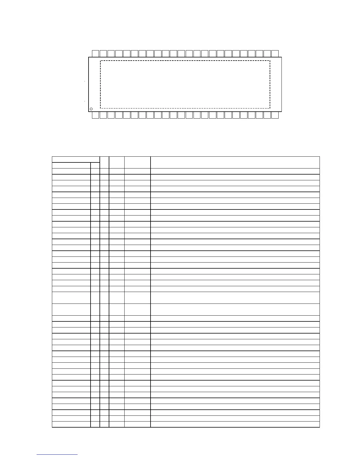
DCA PACKAGE
HTSSOP-48 (12 mm x 8 mm)
(TOP VIEW)
TERMINAL FUNCTIONS
TERMINAL
PULL- 5-V
NAME PIN I/O DOWN TOLERANT DESCRIPTION
RSV2 1 — — — Reserved, tied to analog ground
RSV1 2 — — — Reserved, left open
RSV2 3 — — — Reserved, tied to analog ground
RSV1 4 — — — Reserved, left open
RSV2 5 — — — Reserved, tied to analog ground
LRCK 6 I Yes No Audio data word clock input
BCK 7 I Yes No Audio data bit clock input
DIN1 8 I No No Audio data input for DAC1 and DAC2
DIN2 9 I No No Audio data input for DAC3 and DAC4
DIN3 10 I No No Audio data input for DAC5 and DAC6
DIN4 11 I No No Audio data input for DAC7 and DAC8
6 Submit Documentation Feedback Copyright © 2008–2009, Texas Instruments Incorporated
Product Folder Link(s): PCM1690
 Loading...