A3V56S30FTP
A3V56S40FTP
256M Single Data Rate Synchronous DRAM
Revision 1.1 Mar., 2010
Page 2 / 39
CLK : Master Clock DQM : Output Disable / Write Mask (A3V56S30FTP)
CKE : Clock Enable DQMU,L : Output Disable / Write Mask (A3V56S40FTP)
/CS : Chip Select A0-12 : Address Input
/RAS : Row Address Strobe BA0,1 : Bank Address
/CAS : Column Address Strobe Vdd : Power Supply
/WE : Write Enable VddQ : Power Supply for Output
DQ0-7 : Data I/O (A3V56S30FTP) Vss : Ground
DQ0-15 : Data I/O (A3V56S40FTP) VssQ : Ground for Output
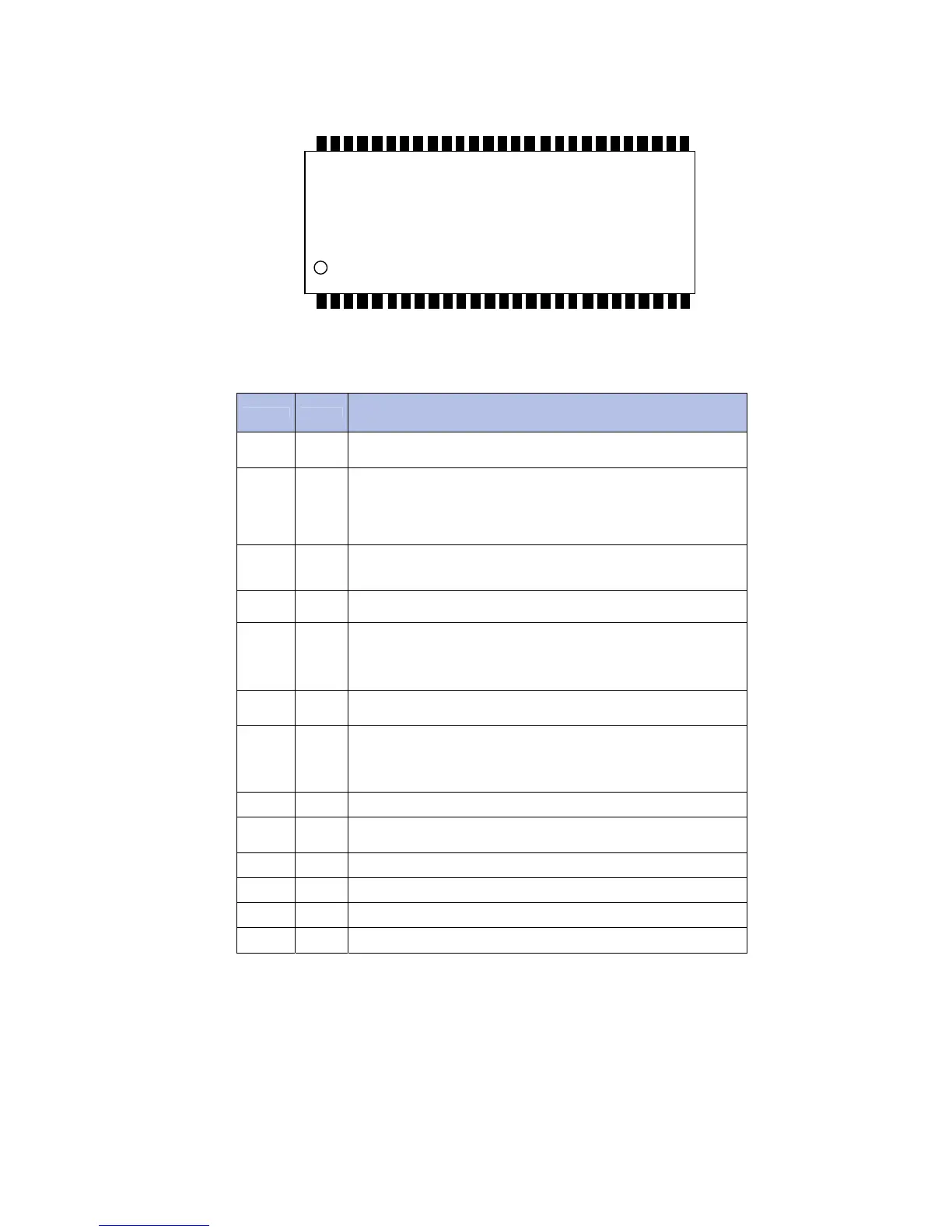
BA0
BA1
Vdd
DQ0
VddQ
Pin Descriptions
SYMBOL TYPE DESCRIPTION
CLK Input
Clock: CLK is driven by the system clock. All SDRAM input signals are sampled on the positive
edge of CLK. CLK also increments the internal burst counter and controls the output registers.
CKE Input
Clock Enable: CKE activates (HIGH) and deactivates (LOW) the CLK signal. Deactivating the
clock provides PRECHARGE POWER-DOWN and SELF REFRESH operation (all banks idle),
ACTIVE POWER-DOWN (row active in any bank), or CLOCK SUSPEND operation (burst /
access in progress). CKE is synchronous except after the device enters self refresh mode, where
CKE becomes asynchronous until after exiting the same mode. The input buffers, including CLK,
are disabled during self refresh mode, providing low standby power. CKE may be tied HIGH.
/CS Input
Chip Select: /CS enables (registered LOW) and disables (registered HIGH) the command
decoder. All commands are masked when /CS is registered HIGH. /CS provides for external
bank selection on systems with multiple banks. /CS is considered part of the command code.
/CAS,
/RAS,
/WE
Input
Command Inputs: /CAS, /RAS, and /WE (along with /CS) define the command being entered.
DQM,
DQML,
DQMU,
Input
Input / Output Mask: DQM is sampled HIGH and is an input mask signal for write accesses and
an output disable signal for read accesses. Input data is masked during a WRITE cycle. The
output buffers are placed in a High-Z state (two-clock latency) when during a READ cycle. DQM
corresponds to DQ0–DQ7 (A3V56S30FTP). DQML corresponds to DQ0–DQ7, DQMU
corresponds to DQ8–DQ15 (A3V56S40FTP).
BA0, BA1 Input
Bank Address Input(s): BA0 and BA1 define to which bank the ACTIVE, READ, WRITE or
PRECHARGE command is being applied.
A0–A12 Input
A0-12 specify the Row / Column Address in conjunction with BA0,1. The Row Address is
specified by A0-12. The Column Address is specified by A0-9(x8) and A0-8(x16). A10 is also
used to indicate precharge option. When A10 is high at a read / write command, an auto
precharge is performed. When A10 is high at a precharge command, all banks are precharged.
DQ0–DQ15 I/O
Data Input / Output: Data bus.
NC –
Internally Not Connected: These could be left unconnected, but it is recommended they be
connected or V
SS.
VddQ Supply
Data Output Power: Provide isolated power to output buffers for improved noise immunity.
VssQ Supply
Data Output Ground: Provide isolated ground to output buffers for improved noise immunity.
Vdd Supply
Power for the input buffers and core logic.
Vss Supply
Ground for the input buffers and core logic.
Vdd
DQ0
VddQ
NC
DQ1
VssQ
NC
DQ2
VddQ
NC
DQ3
VssQ
NC
Vdd
NC
/WE
/CAS
/RAS
/CS
BA0
BA1
A10(AP)
A0
A1
A2
A3
Vdd
Vss
DQ7
VssQ
NC
DQ6
VddQ
NC
DQ5
VssQ
NC
DQ4
VddQ
NC
Vss
NC
DQM
CLK
CKE
A12
A11
A9
A8
A7
A6
A5
A4
Vss
165
 Loading...