Do you have a question about the Denon RCD-N9 and is the answer not in the manual?
Explains the search function in Acrobat Reader for finding references within the manual.
Details how to use the search function to find specific references in diagrams and lists.
Explains how to click connector references to jump directly to their location in schematics.
Instructions on how to use the Sign function to add personal notes to the manual.
Guide to magnifying schematic and circuit board diagrams using keyboard and mouse.
Steps for configuring print settings to output magnified parts of the manual.
Explains using Pan & Zoom to view specific areas of magnified diagrams.
Describes the Loupe Tool for magnifying specific diagram parts in a separate window.
Procedures for leakage current and line-to-chassis resistance checks.
Warnings and precautions regarding electric shock hazards during servicing.
Precautions for safe disassembly and assembly, including handling burrs.
Emphasis on using specified parts, especially those marked for safety.
Guidelines for correct reassembly and wire placement for safety.
Instructions for final safety checks, including insulation testing.
How critical safety parts are indicated by a mark in schematic diagrams.
How critical safety parts are indicated by a mark in parts lists.
Warnings regarding critical parts and pre-return service checks.
Notes on unavailable parts ('nsp') and ordering distinctions.
Instructions for grounding human body and workbench for ESD protection.
Identifies unit as Class 1 Laser Product, requiring qualified personnel.
Warning to avoid direct exposure to the laser beam.
Caution regarding visible/invisible laser radiation when unit covers are open.
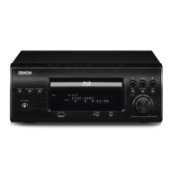
Details specifications for the audio section and CD player functionality.
Technical data for wireless LAN and Bluetooth connectivity.
Specifications for the clock, alarm, and sleep timer functions.
General specifications including power supply and consumption.
Specifies the unit of measurement for physical dimensions as millimeters.
Indicates the weight of the unit as 3.2 kilograms.
Procedure to initialize the unit after replacing microcomputer or digital PCB.
Specifies the measuring discs required for servicing the unit.
Steps and notes for replacing the WLAN module and NFC module.
Refers to the DISASSEMBLY section for detailed part removal steps.
Outlines steps for measuring board test points, including disassembly.
Caution to wait 5 mins after power off before disconnecting SMPS/AMP PCB.
Warning about potential surge current damage to D-AMP IC70 during disconnection.
Procedure for attaching AMP PCB, emphasizing pin alignment to prevent damage.
Warning about IC damage if AMP PCB terminals are misaligned during connection.
Method to protect the LD circuit by soldering before connection.
Guidelines for handling the laser pick-up to prevent dust and damage.
Precautions for grounding and avoiding static electricity during assembly.
Method to check laser pick-up defects via laser drive current in Special Mode.
General instructions for part removal, reassembly, and wire shaping.
Steps and references for disassembling the rear mold panel.
Steps and references for disassembling the side panel.
Steps and references for disassembling the top panel assembly.
Steps and references for disassembling the CD PCB.
Steps and references for disassembling the CD mechanism assembly.
Steps and references for disassembling the Ethernet PCB assembly.
Steps and references for disassembling the shield case.
Steps and references for disassembling the Tuner/Optical PCB.
Steps and references for disassembling the Main PCB.
Steps and references for disassembling the SMPS PCB.
Steps and references for disassembling the Front Panel Assembly.
Steps and references for disassembling the Input PCB.
Steps and references for disassembling the USB PCB.
Explains photo angle indicators and shooting directions used in disassembly.
Detailed steps for removing the rear mold panel.
Shows disassembly sequence and steps for the side panel.
Indicates disassembly sequence and steps for the top panel assembly.
Outlines the disassembly path to reach the CD Mecha Assembly.
Initial steps for CD Mecha disassembly: opening tray and removing door.
Procedure for short-circuiting laser pick-up and disconnecting wires safely.
Shows disassembly sequence to access the Ethernet PCB Assembly.
Steps to remove screws, connector wire, and FFC for Ethernet PCB.
Indicates the disassembly path to reach the CD PCB.
Steps to cut wire clamp and remove wires/FFC for CD PCB.
Outlines the disassembly path to access the Shield Case.
Instruction to remove screws for shield case disassembly.
Shows the disassembly sequence to access the Tuner/Optical PCB.
Steps to remove screws, connector wire, and FFC for Tuner/Optical PCB.
Indicates the disassembly path to reach the Main PCB.
Steps to remove connector wire and screws for Main PCB.
Shows the disassembly sequence to access the SMPS PCB.
Steps to remove screws, support, and connector wire for SMPS PCB.
Outlines the disassembly path to access the Front Panel Assembly.
Instruction to remove screws for Front Panel Assembly disassembly.
Steps to remove connector wire, FFC, and screws for Front Panel Assembly.
Explains how to use buttons to enter various special modes.
Mode to display the firmware version of the unit.
Mode to restore settings to factory defaults, clearing user data.
Mode for user-specific initialization, retaining some data.
Mode for servo adjustment, laser current, and ON time checks.
Mode to display the unit's protection occurrence history.
Mode to switch the unit to USB update mode.
Mode for forcefully switching to USB update mode for recovery.
Details that various settings are initialized, referring to 'Initialization Items'.
Notes on what data is cleared or not cleared during factory initialization.
Step-by-step guide for performing factory initialization.
Table listing settings and their default values after initialization.
Explains that various settings are initialized, referring to 'Initialization Items'.
Highlights differences between user and factory initialization regarding data retention.
Steps for performing user initialization mode.
Procedure for entering Version Display Mode.
Lists the sequence of information displayed in Version Display Mode.
Displays the version of the System u-com.
Displays the version of the System u-com boot loader.
Displays the version of the Network u-com boot loader.
Displays the version of the Network u-com image.
Displays the Bluetooth Mac Address.
Steps to enter and initiate the CD Test Mode.
Instructions on preparing the unit and disc for CD Test Mode.
Procedure for checking servo functions: LD ON, Focus ON, CLV ON.
Waveform display for Tracking ON status in CD Test Mode.
Procedure for reading sub code and checking BER (Block Error Rate).
How to move the pickup using cursor buttons in stop mode.
Procedure for servo on, auto adjustment, and stopping playback.
How to view adjustment values for servos like focus and tracking.
Procedure for measuring and displaying laser current.
Procedure for storing the laser current value in EEPROM.
Displays the total accumulated laser on time.
How to reset the accumulated laser on time count.
Steps to enter Protection History Display Mode.
Indicates that no protection events have been detected.
Shows thermal protection status, indicating D-AMP temperature increase.
Indicates speaker short protection status and condition.
Indicates over-current detection status for the digital amplifier.
Indicates DC protection status for various voltages.
Procedure to reset the protection history.
Notes on replacing NFC module when updating system software.
Steps for updating firmware using a USB memory drive.
Instructions for preparing and connecting the USB memory.
Steps for unzipping the downloaded firmware file on a computer.
Shows the required file structure for the USB memory update.
Important note to remove the LAN cable during firmware updates.
Instructions to start the firmware update process.
Message shown on the display during the USB firmware update process.
Indicates the completion of the firmware update process.
Essential precautions to follow before, during, and after firmware updates.
Explains the purpose of this mode for unit recovery.
Procedure for entering Forced USB All Device Write Mode.
Indicates completion of the forced USB update.
Troubleshooting steps for when the OLED display does not light up.
Checks SMPS PCB power supply voltages as a diagnostic step.
Checks System μ-com power supply voltages.
Verifies the reset signal for the Main μ-com.
Checks the oscillation waveform on the Main PCB.
Verifies power supply voltages for the OLED module.
Checks the drive signals for the OLED module.
Checks signals related to audio output and control.
Verifies digital audio data output from the CODEC.
Verifies digital audio data input to the PWM CONTROLLER.
Checks PWM waveform output from the AMP PCB.
Checks PWM waveforms from specific terminals, including IC70.
Addresses issues with PWM waveform not outputting, checking DIR/PWM controller.
Addresses disrupted PWM waveforms, checking IC70.
Verifies power supply voltages for the DIR component.
Checks power supply voltages for the PWM CONTROLLER AMP PCB.
Verifies power supply voltages for the AMP IC.
Checks the reset signal for the DIR component.
Verifies the reset signal for the PWM CONTROLLER.
Checks the reset signal for the AMP IC.
Checks oscillation waveforms on the Main PCB.
Verifies power supply voltages for the CD PCB.
Checks the reset signal for the CD PCB.
Checks the oscillation waveform on the CD PCB.
Verifies digital audio data for the CODEC on the Main PCB.
Verifies power supply voltages for the TUNER section.
Checks analog audio data output from the TUNER PACK.
Checks the output from the analog selector.
Verifies the DIR input signal.
Checks the analog audio signal from the analog input.
Verifies the DIR input signal.
Verifies power supply voltages for the optical input IC.
Checks digital audio data input from the optical source.
Verifies power supply voltages for the network PCB.
Checks power supply voltages for the front USB PCB.
Verifies power supply voltages for the CY920 module.
Checks the reset signal for the Ethernet PCB (CY920).
Verifies digital audio data for the CODEC on the Network PCB.
General method for checking waveforms using an oscilloscope and ground probe.
Caution regarding measuring discs and HF waveforms.
Lists the discs used for measuring and testing.
Identifies test points on the MAIN PCB and CD PCB for measurement.
Displays the RF waveform (eye-pattern) during CD playback.
Shows waveforms related to CD disc detection.
Displays waveforms related to TOC (Table of Contents) reading.
Shows waveforms related to focus adjustment during CD playback.
Waveform displays for LRCK, SCLK, and SDATA signals during CD playback.
Waveforms for OPSW, FCLSW, LOAD-, and LOAD+ signals.
Block diagram of the Top Key Board components.
Block diagram of the CD Board components.
Block diagram of the Network Board components.
Block diagram of the Front Board components.
Block diagram of the Switched-Mode Power Supply.
Block diagram of the Main Board components.
Block diagram of the Amplifier Board components.
Power block diagram illustrating power distribution and regulation for the unit.
Power states related to normal operation of the unit.
Power states associated with network, OLED, and normal standby modes.
Power control related to audio, network, OLED, and VBUS functions.
Wiring diagram for the Tuner and Optical Jack PCB.
Wiring diagram for the Network PCB.
Wiring diagram for the Front PCB.
Wiring diagram for the Key PCB.
Wiring diagram for the Amplifier PCB.
Wiring diagram for the Main PCB.
Wiring diagram for the CD PCB.
Wiring diagram for the SMPS PCB.
Note on using lead-free solder for soldering components.
Printed wiring board layout for the HP section (A & B sides).
Printed wiring board layout for the Tuner Digital section (A & B sides).
Printed wiring board layout for the CD section (A & B sides).
Printed wiring board layout for the Key section (A & B sides).
Printed wiring board layout for the Front section (A & B sides).
Printed wiring board layout for the SMPS section (A & B sides).
Printed wiring board layout for the Main section (A & B sides).
Printed wiring board layout for the D-AMP section (A & B sides).
Printed wiring board layout for the Network/WiFi section (A & B sides).
Printed wiring board layout for the USB section (A & B sides).
Printed wiring board layout for the AC Inlet section (A & B sides).
Schematic diagram for the MCU and DSP sections.
Schematic diagram for the Network and Wi-Fi circuitry.
Schematic diagram for the CD playback circuitry.
Schematic diagram for the Digital Amplifier section.
Schematic diagram for the Front Panel and associated components.
Schematic diagram for the Switched-Mode Power Supply.
Indicates that the complete part list is found in the final chapter.
Warning about critical parts requiring manufacturer-specified replacements.
Directs the user to the final chapter for the part list.
Notes that only major semiconductors are listed, omitting general ones.
Lists integrated circuits (ICs), specifically R5F56108VNFP (MAIN : IC28).
Details pin functions and behavior across standby modes for R5F56108VNFP.
Provides specific notes and functions for each pin of the R5F56108VNFP IC.
Continues detailing pin functions and behavior across standby modes for R5F56108VNFP.
Continues notes and functions for each pin of the R5F56108VNFP IC.
Continues detailing pin functions and behavior across standby modes for R5F56108VNFP.
Continues notes and functions for each pin of the R5F56108VNFP IC.
Block diagram illustrating the internal structure of the TC94A92FG IC.
List of pin numbers for the TC94A92FG IC.
List of symbols for each pin of the TC94A92FG IC.
Specifies the input/output mode for each pin.
Detailed description of each pin's function.
Default state or value for each pin.
Additional remarks or connection notes for pins.
Continues the list of pin numbers for the TC94A92FG IC.
Continues the list of symbols for each pin of the TC94A92FG IC.
Continues input/output mode specifications for pins.
Continues detailed descriptions of pin functions.
Continues default states or values for pins.
Continues additional remarks or connection notes for pins.
Details pin functions for the IP4001CR IC used in CD section.
Pin number list for IP4001CR.
Pin symbols for IP4001CR.
Input/Output mode for IP4001CR pins.
Detailed pin descriptions for IP4001CR.
Block diagram showing the internal structure and signal flow of PCM9211.
List of pin numbers for the PCM9211 IC.
List of pin names for the PCM9211 IC.
Input/Output mode for PCM9211 pins.
Indicates if pins are tolerant to 5V signals.
Detailed description of each pin's function for PCM9211.
Pin configuration for the NJM2752 IC.
List of pin numbers for the NJM2752 IC.
List of symbols for each pin of the NJM2752 IC.
Detailed function description for each pin of the NJM2752 IC.
Block diagram of the NJM2755, related to the audio switch.
Details pin functions for the TAS5142DKD IC used in the amplifier.
List of terminal names for the TAS5142DKD IC.
DKD numbering for TAS5142DKD pins.
DDV numbering for TAS5142DKD pins.
Functional description for TAS5142DKD pins.
Detailed description of TAS5142DKD pin functions.
Block diagram illustrating the internal structure of the TAS5142 IC.
Details pin functions for the TAS5558 IC.
List of pin numbers for the TAS5558 IC.
List of pin names for the TAS5558 IC.
Type of signal (Analog, Digital, Power) for TAS5558 pins.
Indicates if TAS5558 pins are 5V tolerant.
Termination details (Pullup, Pulldown) for TAS5558 pins.
Detailed description of TAS5558 pin functions.
Block diagram illustrating the internal structure and signal flow of TAS5558.
Details pin functions for the EN5339QI ICs used in the network section.
List of pin names for the EN5339QI ICs.
Detailed function description for each pin of the EN5339QI ICs.
Block diagram of the EN5339QI IC, showing its internal functions.
Details pin functions for the MX25L25635FMI Flash Memory IC.
List of symbols for each pin of the MX25L25635FMI IC.
Detailed function description for each pin of the MX25L25635FMI IC.
Important notes regarding RESET# pin and DNU/SIO3 pin usage.
Block diagram of the MX25L25635FMI IC, showing its internal structure.
Block diagram of the TC7USB40MU USB switch IC.
Details pin functions for the TPC6111 MOSFET.
Details pin functions for the ICE3BS03LJG SMPS controller IC.
List of symbols for each pin of the ICE3BS03LJG IC.
Detailed function description for each pin of the ICE3BS03LJG IC.
Block diagram of the ICE3BS03LJG SMPS controller IC.
Details pin functions for the NR111E SMPS controller IC.
List of pin numbers for the NR111E IC.
List of symbols for each pin of the NR111E IC.
Detailed function description for each pin of the NR111E IC.
Block diagram of the NR111E SMPS controller IC.
Details pin functions for the S020-MXS4035A-3 OLED display module.
List of pin numbers for the display module.
List of pin names for the display module.
Input/Output mode for display module pins.
Detailed function description for each pin of the display module.
Note that parts marked 'nsp' are not available for supply.
States parts are for maintenance and may differ in appearance/dimensions.
Explains symbols in the Remarks column indicating model destinations.
Reference numbers for components on the Front PCB.
Component list for semiconductors on the Front PCB.
Component list for resistors on the Front PCB.
Component list for capacitors on the Front PCB.
Component list for miscellaneous parts on the Front PCB.
Note that parts marked 'nsp' are not available for supply.
States parts are for maintenance and may differ in appearance/dimensions.
Explains symbols in the Remarks column indicating model destinations.
Reference numbers for components on the Main PCB.
Component list for semiconductors on the Main PCB.
Component list for resistors on the Main PCB.
Component list for capacitors on the Main PCB.
Component list for miscellaneous parts on the Main PCB.
Note that parts marked 'nsp' are not available for supply.
States parts are for maintenance and may differ in appearance/dimensions.
Explains symbols in the Remarks column indicating model destinations.
Reference numbers for components on the DAMP PCB.
Component list for semiconductors on the DAMP PCB.
Component list for resistors on the DAMP PCB.
Component list for capacitors on the DAMP PCB.
Component list for miscellaneous parts on the DAMP PCB.
Note that parts marked 'nsp' are not available for supply.
States parts are for maintenance and may differ in appearance/dimensions.
Explains symbols in the Remarks column indicating model destinations.
Reference numbers for components on the CD PCB.
Component list for semiconductors on the CD PCB.
Component list for resistors on the CD PCB.
Component list for capacitors on the CD PCB.
Component list for miscellaneous parts on the CD PCB.
Note that parts marked 'nsp' are not available for supply.
States parts are for maintenance and may differ in appearance/dimensions.
Explains symbols in the Remarks column indicating model destinations.
Reference numbers for parts in the exploded view.
Part numbers for components in the exploded view.
Names of components in the exploded view.
Remarks about components in the exploded view.
Quantity of components in the exploded view.
New version information for components in the exploded view.
Note that parts marked 'nsp' are not available for supply.
States parts are for maintenance and may differ in appearance/dimensions.
Explains symbols in the Remarks column indicating model destinations.
Reference numbers for packing items.
Part numbers for packing items.
Names of packing items.
Remarks about packing items.
Quantity of packing items.
New version information for packing items.
| Security algorithms | WPS |
|---|---|
| Supported radio bands | AM, FM |
| Built-in storage media | - |
| Audio formats supported | AAC, AIFF, FLAC, MP3, WAV, WMA |
| Smartphone remote support | Yes |
| Internet radio services supported | iDevice, iTunes |
| Product color | Black |
| Wi-Fi standards | 802.11b, 802.11g, Wi-Fi 4 (802.11n) |
| Digital audio optical out | 1 |
| Apple docking compatibility | iPhone, iPod |
| Power consumption (typical) | 55 W |
| Depth | 305 mm |
|---|---|
| Width | 280 mm |
| Height | 102 mm |
| Weight | 3300 g |