About the development board Connectors and blocks
Digi Connect ME, Wi-ME, ME 9210, Wi-ME 9210 Hardware Reference Manual
28
JTAG Debugger Connector Pin Assignments
Pin 1 Pin 2 Pin 3 Pin 4 Pin 5 Pin 6 Pin 7 Pin 8 Pin 9 Pin 10
VCC+ VCC+ /TRST GND TDI GND TMS GND TCK GND
Pin 11 Pin 12 Pin 13 Pin 14 Pin 15 Pin 16 Pin 17 Pin 18 Pin 19 Pin 20
RTCK GNO TDO GND /SRST GNO N/A GND N/A GND
Note Pin assignments are shown for the connector on the development board.
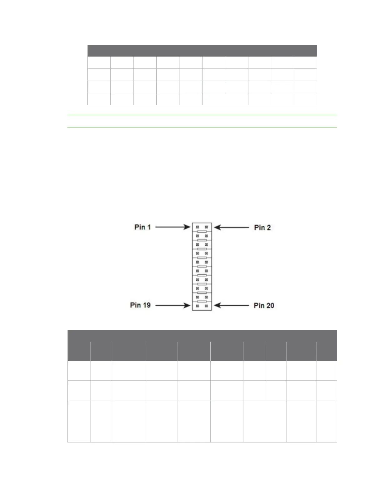
Logic analyzer header, P3
The Logic Analyzer Header is a 20-pin male vertical header that is labeled P3 on the development
board. The header is for connecting a digital signal analyzer (for example, a logic analyzer) to the
development board. See the following figure for pin orientation; see the following table for pin
assignments.
The figure shows the connector using the same orientation as shown in the figure titled Board layout
and connector locations.
Logic analyzer header pin orientation
Logic Analyzer Header Pin Assignments
Pin 1 Pin 2 Pin 3 Pin 4 Pin 5 Pin 6 Pin 7 Pin 8 Pin 9
Pin
10
V_
Ether+
V_
Ether-
Not
connected
Not
connected
Not
connected
Not
connected
RXD TXD GPIO-4 GPIO-
5
Pin 11 Pin 12 Pin 13 Pin 14 Pin 15 Pin 16 Pin 17 Pin 18 Pin 19 Pin
20
GPIO-
2
GPIO-
3
GPIO-1 /RST 3.3v GND See Power
and device
interface
connector for
details.
Reserved /INIT
 Loading...