Basys MX3™ Board Reference Manual
Copyright Digilent, Inc. All rights reserved.
Other product and company names mentioned may be trademarks of their respective owners.
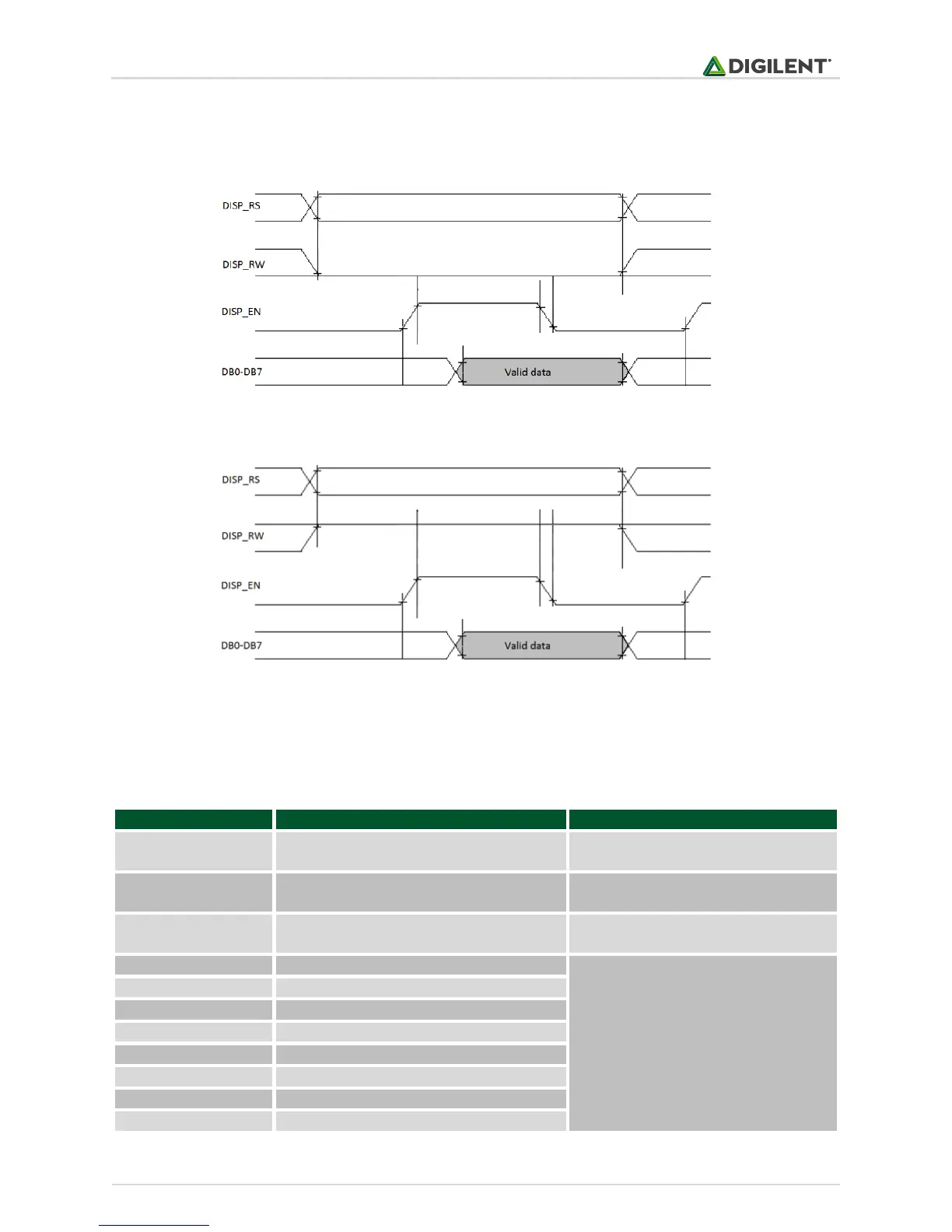
The following timing diagrams detail how write and read processes must be implemented. The essential difference
is the polarity of the DISP_RW signal (0 for write and 1 for read). For more detailed timing information, refer to the
KS0066U datasheet.
Figure 8.2. LCD write timing.
Figure 8.3. LCD read timing.
8.1 Connectivity
AN15/RPB15/OCFB/CTED6/PMA0/RB15
Register Select: High for Data Transfer,
Low for Instruction Transfer.
Read/Write signal: High for Read
mode, Low for Write mode.
Read/Write Enable: High for Read,
falling edge writes data
Table 8.1. LCD connectivity.