EasyManua.ls Logo

Digilent Basys MX3 - Appendix 3: Basys MX3 Pinout

Digilent Basys MX3
56 pages
Print Icon
To Next Page IconTo Next Page
To Previous Page IconTo Previous Page
Loading...
Basys MX3™ Board Reference Manual
Page 53 of 56
Appendix 3: Basys MX3 Pinout
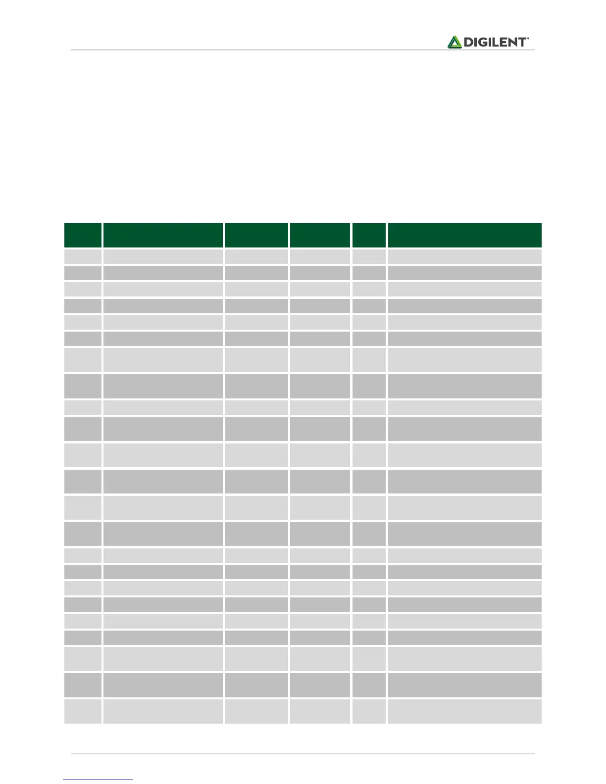
The following table details the Basys MX3 pinout, showing the following information:
Pin #, Full Pin Name: The number and the name of the microcontroller pin, as in the microcontroller
datasheet pin.
Peripheral: The Basys MX3 peripheral that uses this pin.
Schematic Name: the name of the pin in the schematic.
PPS: The PPS remapping function of this pin.
Function: The available function(s) of this pin.
Pin #
Full Pin Name
Peripheral
Schematic
Name
PPS
Function
1
RG15
SSD
CE
RG15
2
VDD
POWER
VCC3V3
3
AN22/RPE5/PMD5/RE5
LCD
DB5
I/O
PMD5
4
AN23/PMD6/RE6
LCD
DB6
PMD6
5
AN27/PMD7/RE7
LCD
DB7
PMD7
6
RPC1/RC1
PMOD
JA2
I/O
SDO2/U3TX/IC3/T2CK/INT3/OC3
7
RPC2/RC2
PMOD
JA1
I/O
SS2/U3CTS/IC1/T3CK/INT1/OC1/O
C2
8
RPC3/RC3
PMOD
JA7
I/O
INT2/U1CTS/U2CTS/IC2/IC5/T4CK/
OC5
9
RPC4/CTED7/RC4
PMOD
JA3
I/O
SDI2/U3RX/IC4/T5CK/INT4/OC4
10
AN16/C1IND/RPG6/SCK2/
PMA5/RG6
PMOD
JA4
I/O
SCK2/U3RTS/IC2/IC5/T4CK/INT2/O
C5
11
AN17/C1INC/RPG7/PMA4
/RG7
PMOD
JA8
I/O
INT4/U1TX/U2TX/IC4/T5CK/OC4
12
AN18/C2IND/RPG8/PMA3
/RG8
PMOD
JA9
I/O
IC3/T2CK/INT3/U1RX/U2RX/OC3
13
MCLR
PROGRAM/
DEBUG
PIC32_MCL
R
14
AN19/C2INC/RPG9/PMA2
/RG9
PMOD
JA10
I/O
IC1/T3CK/INT1/U1RTS/U2RTS/OC1
/OC2
15
VSS
POWER
GND
16
VDD
POWER
VCC3V3
17
TMS/CTED1/RA0
LEDS
LED0
RA0
18
RPE8/RE8
MOTOR
AIN2
I/O
OC2/RE8
19
RPE9/RE9
MOTOR
BIN1
I/O
OC5/RE9
20
AN5/C1INA/RPB5/RB5
MOTOR
BIN2
I/O
OC3/RB5
21
AN4/C1INB/RB4
MICROPHO
NE
A_MIC
AN4/C1INB
22
PGED3/AN3/C2INA/RPB3/
RB3
MOTOR
AIN1
I/O
OC4/RB3
23
PGEC3/AN2/C2INB/RPB2/
CTED13/RB2
POTENTIOM
ETER
AIC
I/O
AN2/C2INB