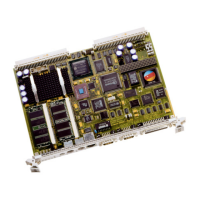
The ELTEC BAB 740 is a Basic Automation Board with a PowerPC 740, designed for various automation and control applications. This manual, revision 2C, provides comprehensive information on its specifications, installation, operation, and maintenance.
Function Description
The BAB 740 serves as a versatile automation board, leveraging a PowerPC CPU for high-performance processing in embedded systems. It integrates a VMEbus interface, allowing it to be used in VMEbus-based systems and expanded with PMC daughter cards. The board supports various I/O options, including serial, parallel, Ethernet, and SCSI, making it adaptable to a wide range of industrial and control environments. Its design emphasizes flexibility and expandability, catering to complex automation tasks. The board's software compatibility with OS-9 and VxWorks further enhances its utility in real-time operating system applications.
Important Technical Specifications
1. Main Features:
- VMEbus: Two PMC daughter card slots (optional), VMEbus slots used.
- PowerPC CPU: 740 with 266 MHz.
- RAM: 8.256 MB DRAM (2 * 64-bit SO DIMMs) EDO/SDRAM 50ns.
- Cache: 512KB on-board.
- PCI Host Bridge: Motorola MPC106.
- PCI-ISA-Bridge: W83C553.
- PCI-to-VME Bridge: Universe II for fast, global VMEbus transfers, decoupled from board-internal PCI transfers.
- Flash EPROM: 2 MB on-board, Flash programmable, byte access implemented in hardware.
- Network Interface: Ethernet using DEC21143 (10/100 Mbps) with PCI-DMA, 10BaseT connector at front panel.
- Serial Synchronous (optional): 2 * RS422 / 3 Mb/s synchronous using Zilog 85230 ESCC.
- Serial Asynchronous: 2 * RS232 with PC97307.
- Real-time Clock: MK48T59.
- SCSI (optional): Symbios 860.
- OS-9 Operating System: Operating system with FasTrak cross development system. VxWorks operating system with Tornado cross development system.
- I/O-compatible: with BAB-40/60 where applicable.
2. CPU Kernel (PowerPC 740):
- Clock rates of 266 MHz and host bus clocks of 66 MHz.
- Contains two parallel 32-bit integer execution units with an additional floating point unit for 8 SPECint95 and 6.2 SPECfp95 at 200 MHz.
- External second-level cache (2-1-1-1 clocks) and main memory attached directly to the CPU's host bus.
- Memory is controlled by the host bridge MPC106, which contains the bridge between host bus and on-board PCI.
- Memory interface for EDO or SDRAM modules in SO DIMM format (144-pin SO DIMM modules; 64-bit data bus).
- Memory size can be anywhere between 8 and 128 MB, depending on the DIMM modules used. Two sockets can be equipped with SO DIMM modules, but the board runs with only one module.
3. Flash Memory:
- Up to 2 MB of user flash memory for storing user-generated programs.
- Diskless systems can be built.
4. PCI Devices:
- Board-internal PCI bus is used for all I/O devices as well as the PCI-to-VME bridge.
- PCI bus is of the master/slave type, capable of DMA transfers as source and target.
- Two single-size PMC slots allow for flexible interfacing, e.g., using a VGA display adapter PMC module and additionally a frame grabber interface.
- Bus-master DMA capabilities of the PMC implementation of the PCI standard, frame grabber can be implemented efficiently without frame buffers.
5. VMEbus Interface (Universe II bridge controller):
- Connects internal PCI bus and external VMEbus.
- Supports 8-, 16-, and 32-bit data transfers in master and slave mode.
- Bus controller (arbiter) functionality is available.
- Can operate without VMEbus; only power must be supplied through VME connectors.
6. Mechanical:
- Double Eurocard (6HU) using two VMEbus slots.
- VMEbus connectors are mounted at the position of the second VMEbus slot (the slot on the right) if two slots are used.
- Two slots for single-size PMC modules are available.
7. I/O:
- 8-bit SCSI routed over the VME P2 connector.
- Serial I/O channels 2 ... 4 and the parallel I/O are also routed via P2.
- Front panel 10BaseT Ethernet connector is located as well as the separate front panel for PMC I/O signals.
- Keyboard connector and two serial RS232 channel are also routed to the front panel (9-pin D connector).
8. Software:
- Standard operating system is OS-9/VxWorks for the PowerPC.
- Development environment is FasTrak for Windows, so that the user can write and debug programs on Windows 95 or Windows NT platform.
- Debug and program download can be done via Ethernet or through the PCI bus.
- BIOS functionality is supplied in the form of the boot program, used to start the operating system OS-9/VxWorks.
- Contains power-on self test routines and PCI device address setup.
9. Compatibility:
- Designed to be software-compatible to the PowerPC reference platform ("Yellowknife").
10. Board Parameters:
- Host Bus: 66MHz.
- VMEbus Master/Slave Capabilities: Single cycle (A16/A24/A32/A64:D08(EO)/D16/D32/UAT A40:D08(EO)/D16/MD32), RMW (Master only: A16/A24/A32:D08(EO)/D16/D32 A40:D08(EO)/D16/MD32), BLT (A24/A32/A64:D08(EO)/D16/D32 A40:D08(EO)/D16/MD32), MBLT (A24/A32/A64:D64), ADO (A16/A24/A32/A40/A64/CR/CSR), ADOH (A16/A24/A32/A40/A64).
- System Controller Options: Arbiter (BTO(16/32/64), forever, IACK daisy-chain driver, SYSCLK driver), Arbiter Options (PRI, RRS, SGL, BBSY filter), Requester Options (Any one of BR(0-3), RWD, ROR, ROC, Bus ownership timer 16 µs... 1024 µs, forever), Interrupt Handler Options (IH(1-7), D08(O), D16, D32), Interrupter Options (I(1-7), D08(O), D16, D32), Auto Configuration (FSD, ASI).
- Address Range: Four PCI target/VME master windows (base and size programmable, 64 KB to 4 GB window size, any of specified address capabilities or user-defined). Four VME slave/PCI initiator windows (base and size programmable, 64 KB to 4 GB window size, any of specified address capabilities or user-defined).
- PCI Local Bus: CPU to PCI Transfer Options (Write post buffer, Max. 120 MB/s (peak)), PCI to Memory Transfer Options (Max. 120 MB/s (peak)), Clock Speed (33.3 MHz), IRQs (Four PCI interrupts rerouted to selectable ISA interrupts).
- Network: 10BaseT/100BaseTx (twisted-pair), Transfer Speed (max. 10/100 Mbit/s).
- SCSI: Ultra SCSI (8 bit), Transfer Speed (asynchronous transfer 7 MB/s, synchronous transfer 20 MB/s (ultra SCSI)).
- Serial I/O: 2 Channels (PC97307): Full duplex, asynchronous, 50 b/s - 115,2 KB/s, RS232 level. 2 Channels (Z85230 ESCC): Full duplex, 50 b/s - 230,4 KB/s asynchronous, up to 3 MB/s synchronous, RS232 or RS422 level.
- Keyboard: MF2/AT mode, PS/2 mode.
- Mouse: PS/2 mode, Serial mouse at channel 1 or channel 2.
- Parallel I/O: Centronics bidirectional, unbuffered TTL, Transfer Rate (max. 2 MB/s).
- MTBF Values: Includes one 64 Mbyte SODIMM: 18900 h (computed after MIL HDBK-217E), 253270 h (realistic value from industry stand experience).
- ESD Values: 2 kV (Human body method).
- Environmental Conditions: Storage Temperature (-40° C - +70° C (non condensing)), Operating Temperature (0° C - +50° C (1 m/s forced air cooling)).
- Maximum Operating Humidity: 85% relative.
- Power Requirements (without PCI extensions): 3,8 A max. 3.0 A typ. +5 VDC +/-5%, 100 mA max. 30 mA typ. +12 VDC +/-10%, 100 mA max. 10 mA typ. -12 VDC +/-10%.
- Battery: Type M4T28-BR12SH1, Approx. 8 years life time.
Usage Features
1. Installation:
- VMEbus Installation: The BAB 740 requires two VMEbus slots. Due to the power dissipation of the MPC740 CPU, it is not recommended to operate the BAB 740 without forced air cooling. The board is designed to be installed carefully and simultaneously with PMC daughter cards (BAB 740 and PMCE).
- SODIMM Installation: Supports 144-pin SO-DIMMs up to 64 Mbyte and some 128 Mbyte SO-DIMMs that fit into X701 and X702. The firmware reads the type and size of the SO-DIMM from the SPD (Serial Presence Detect) EEPROM installed on the memory module. SDRAMs should be 100 MHz or faster. FPMODE or EDO RAMs should be 60 ns or faster. X701 must be populated with a memory module. If two memory modules are installed, they should be of the same type but may have different size. The firmware uses only the module installed in X701. Due to performance reasons, the use of SDRAM is strongly recommended (50% advantage). After reset, the firmware tests the memory modules. If the test fails or the firmware reports the wrong size, the module may not be suitable for the BAB 740.
- Activity LEDs: Four activity LEDs on the front panel provide visual status indications:
- RUN (Green): CPU data bus in usage.
- DISK (Yellow): Access to IDE or SCSI bus.
- LINK (Green/Yellow): Green = 100 Mbit link pulses present, Yellow = 10 Mbit link pulses present.
- ACT (Yellow): Network activity.
- Booting: The board can boot from a boot screen printout, OS-9, or via Ethernet using the BOOTP protocol. Boot parameters can be entered for OS-9. The BOOTP server must send the response directly to the BAB 740; broadcasts are not analyzed.
2. Connector Assignments:
- Keyboard and Mouse Connector: 6-pin miniature circular connectors for KBDATA, GND, +5V, and MCLK.
- Ethernet Connector: 8-pin telephone jack connector for TXD+, TXD-, RXD+, RXD-.
- Serial Ports 1 and 2 Connectors: 9-pin min-D connector for DCD, RXD, TXD, DTR, GND, DSR, RTS, CTS, RI.
- Parallel I/O Connector: 25-pin min-D connector for /STROBE, D0-D8, /ACK, BUSY, PE (Paper End), /SLCT, /AUTO FEED, /ERROR, /INIT, /SLCT IN, GND.
- VMEbus Connector P1 (X2001): 32-pin connector with various signals including D00-D31, /BBSY, /ACFAIL, /BG0IN, /BG0OUT, /BG1IN, /BG1OUT, /BG2IN, /BG2OUT, /BG3IN, /BG3OUT, /BR0-BR3, /WRITE, /DTACK, AM0-AM5, GND, /IACK, /IACKOUT, A07-A31, /IRQ0-IRQ7, +12V, -12V, +5V. Signals in parentheses are not connected.
- VMEbus Connector P2 (X2002): 32-pin connector with signals for SCSI, IDE, and C3/C4 I/O. Lines on rows A and C are TTL-level, except Cx signals which have RS 232C level (SILC-200 used). Pin assignment changes for RS 422 configuration. Row B is reserved for 32-bit VMEbus extension.
- ADAP-200 Connectors:
- 8-bit SCSI (X103): 50-pin connector for SCSI signals. J1601 must be installed for signal termination. All odd pins of the 50-pin SCSI connector except pin 25 are connected to ground. Pin 25 is left open. Pin 26 is connected to +5 V via a Schottky diode to supply power to an external SCSI terminator.
- 50-Pin I/O Connector (X102): For additional serial channels (Channel 3 and 4) and reserved pins.
- CONV-300 Connectors:
- COM3, COM4 (9-pin min-D connector): For RS232 and RS422 asynchronous/synchronous signals.
- ADAP-740 Connectors:
- Floppy Disk (X101): 34-pin connector for floppy drive and adapter.
- EIDE (X105): 40-pin connector for EIDE drives (harddisk, CD-ROM). Cable length should not exceed 40 cm to avoid instable operation. EIDE is only available on board versions with EIDE option.
- COM3 and COM4 (X103 and X104): The pinout of X103 and X104 on ADAP-740 is such that a crimped cable with a 10 pin edge connector and a 9 pin Min-D male connector results in the same pinout as Table 11.
- Speaker (X106): 4-pin connector for speaker.
- PMCE-740 Connectors:
- VMEbus Connector P1 (X402): Only GND, +5V and +12V are routed from the VMEbus Connector P1 to the Power Connector X403. No VMEbus Signals are used.
- PCI Mezzanine Card Connectors (Jn11, Jn12, Jn21, Jn22 (X101, X102, X201, X202)): These connectors route the PMCE I/O to the VMEbus P2 Connector.
- Power Connector (X403): Provides +5V out, GND, and +12V out.
3. Jumpers:
- On-board Jumpers:
- Boot ROM Select (J114): Open for Boot from Boot-ROM, Short for Boot from User-ROM (default).
- SCSI Termination (J1601): Open to disable termination, Short to enable termination (default).
- SMI Interrupt Routing (J1701): Routes no SMI interrupt, Universe INT0 to SMI, Universe INT0 to SMI, Universe INT0 to SMI, SMITICK to SMI (default).
- Universe PCI Interrupt Routing (J1702...J1705): Routes Universe INT0, INT1, INT2, INT3, INT4, INT5, INT6, INT7 to PCI IRQ A, B, C, D.
- VMEbus SYSRESET (J1706, J1902): Short J1706 for no VMEbus SYSRESET, Short J1902 for VMEbus SYSRESET is input, Short J1706 and J1902 for VMEbus SYSRESET is output (default), Not allowed for both open.
- VMEbus SYSFAIL (J1901): Open for no VMEbus SYSFAIL, Short for VMEbus SYSFAIL output enable (default).
- COM3 Configuration (J2201, J2202, X2201) and COM4 Configuration (J2203, J2204, X2202): Configure RS232 or RS422 async. (default) using SILC-200 or SILC-300.
- PMCE-740 Jumpers:
- PMC Slot 1 PCIREQ and PCIGNT Routing (J201): 1-2 to use PCIREQ, PCIGNT of PMC Slot 0, 3-4 to use PCIREQ, PCIGNT of BAB 740 Onboard SCSI Controller. Warning: PCIREQ and PCIGNT of PMC Slot 0 or SCSI Controller can only be used if the corresponding device is not equipped!
- PMC Slot 1 Interrupt Routing (J204): Routes PMC IRQ A to PCI IRQ A, B, C, D.
Maintenance Features
1. General Safety Information:
- Electrical Safety: To prevent electrical shock hazard, disconnect the power cable from the electrical outlet before reloading the system.
- Adding/Removing Devices: When adding or removing devices to or from the system, ensure that the power cables for the devices are unplugged before the signal cables are connected. If possible, disconnect all power cables from the existing system before you add a device.
- Connecting/Removing Signal Cables: Before connecting or removing signal cables from the motherboard, ensure that all power cables are unplugged.
- Power Supply: Make sure that your power supply is set to the correct voltage in your area. If you are not sure about the voltage of the electrical outlet you are using, contact your local power company.
- Power Supply Issues: If the power supply is broken, do not try to fix it yourself. Contact a qualified service technician or your retailer.
2. Operation Safety:
- Installation: Before installing the motherboard and adding devices on it, carefully read the manuals that came with the package.
- Product Handling: Before using the product, make sure all cables are correctly connected and the power cables are not damaged. If you detect any damage, contact your dealer immediately.
- Short Circuits: To avoid short circuits, keep paper clips, screws, and staples away from connectors, slots, sockets, and circuitry.
- Environmental Conditions: Avoid dust, humidity, and temperature extremes. Do not place the product in any area where it may become wet.
- Placement: Place the product on a stable surface.
- Technical Problems: If you encounter technical problems with the product, contact a qualified service technician or your retailer.
3. EMC Rules:
- This unit must be installed in a shielded housing.
- If not installed in a properly shielded enclosure, and used in accordance with the instruction manual, this product may cause radio interference.
- In which case the user may be required to take adequate measures at his or her own expense.
4. Important Information:
- This product is not an end user product. It was developed and manufactured for further processing by trained personnel.
5. Recycling:
- Packaging: Please recycle packaging environmentally friendly. Packaging materials are recyclable. Please do not dispose of packaging into domestic waste but recycle it.
- Old/Redundant Devices: Please recycle old or redundant devices environmentally friendly. Old devices contain valuable recyclable materials that should be reutilized. Therefore, please dispose of old devices at collection points which are suitable.
6. Appendix - Description of On-board Devices:
- SMI Ticker: The output of counter/timer 2 of the W83C553F may be routed to the System Management Interrupt input of the CPU when J1701 is set to position 7-8. This can be used to generate a periodic interrupt with higher priority than normal interrupts. A negative edge of the PC-Speaker output triggers the SMI when enabled via bit 7 of I/O address $809. Writing to I/O address $808 clears the SMI.
- Enhanced Serial Communications Controller (ESCC): Two serial controllers COM1 and COM2 are incorporated in the PC97307 Super-I/O. The BAB 740 features another two serial lines that are realized with a Z85230 ESCC. The ESCC is clocked with 12 MHz or 14.7456 MHz. This allows transfer rates up to 3 MBaud synchronous and 230.4 KBaud asynchronous. Channel A can be operated with DMA to reduce interrupt load of the CPU for synchronous block protocols. DMA channel 0 is used for receive and Channel 1 for transmit. The DMA controller must be programmed to type A or B mode. The Interrupt request of the ESCC is connected to INT9 input of the interrupt controller.
- Interrupt Controller: The on-board interrupt sources are connected to the interrupt controller, located logically in the W83C553 chip. This chip then prioritizes and drives the two CPU interrupt inputs.
- SRAM/RTC: An indirect addressing scheme is used to access the M48T59Y SRAM/RTC. To access the SRAM/RTC, the desired address first must be written to I/O address $70 and $71. Then the data can be accessed via I/O address $76. The interrupt output of the M48T59Y is connected with the INT5 input of the interrupt controller. It may be used to generate periodic interrupts or watchdog interrupts.
- GPIO Use: The GPIOs of the Super-I/O are used for various purposes, including CPU Bus Speed, L2 Cache Size, I2C Clock for SPD of 1st/2nd SODIMM, I2C Data for SPD of 1st/2nd SODIMM, HEX Switch LSB/MSB, and others.
- Super-I/O Power-on Strappings: The Super-I/O wakes up in the following configuration: CFG0 (FDC, KBC and RTC inactive), CFG1 (No X-Bus Data Buffer), CFG3,2 (Clock source is 24 MHz fed via X1 Pin), BADDR1,0 (Print Motherboard, Wake in Config state, Index 015Ch), SELCS (/CS0 on /CS0 pin).
- I/O Address Map: Provides a detailed map of I/O addresses for various devices like DMA Controller, Interrupt Controller, Counter/Timer, Keyboard Data, Port B, SRAM/RTC, BIOS Timer, DMA Page, PCI Bus, SuperI/O, Parallel Port, COM ports, Floppy, VGA Controller, Interrupt Mode, SMI Status Register, SMI Control Register, ESCC Channel A/B Control/Data.
- Memory Address Map: Describes how the BAB 740 uses address map B (CHRP) of the MPC106.
- PCI IDSEL: The IDSEL input of each PCI device is connected to one of the PCI address/data lines for individual addressing in configuration space.
- Factory-settable Jumpers: Includes CPU Drive Strength Configuration (J101, J102), CPU PLL Configuration (J103...J106), System Clock (J111, J112, J113), MPC106 PLL Configuration (J110...J107), Cache Size (J601, J602, J603), Hardware Debugger Configuration (J1301), and Revision EEPROM Write Protection (J1302). SMD jumpers are for factory use only. Note: Implementation specific settings; do not change!