7
2.5 Installation layout
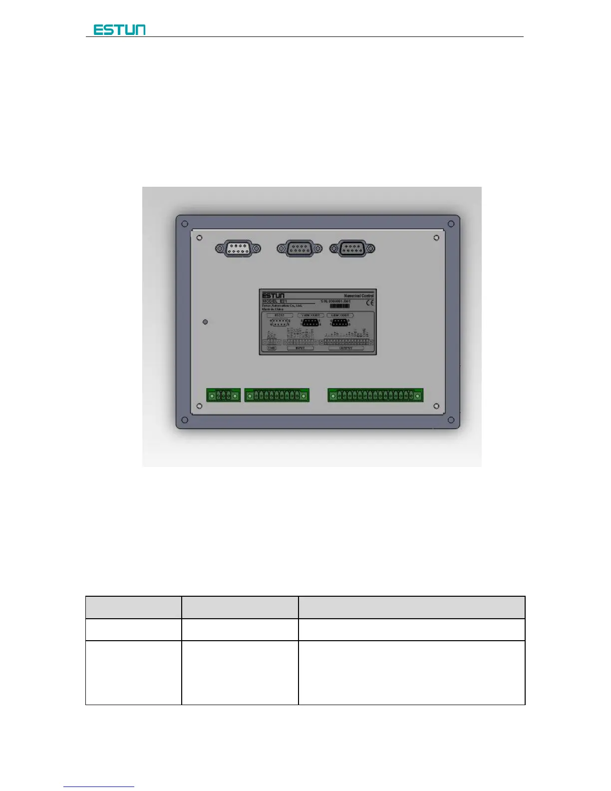
2.5.1 Layout of rear panel
Rear panel block diagram is as shown in Figure 2-2, consisting of power port
(POWER), input port (INPUT), output port (OUTPUT), encoder port (X, Y), and
communication port (COMM).
Figure 2-2 Rear panel layout
2.5.2 Rear panel port description
Rear panel port description is as shown in Table 2-1.
Table 2-1 Rear panel port description
13 pin. 24VDC, maximum drive capability 70mA,
opto-coupler isolation, maximum withstanding
voltage 40V.