3 Application Interfaces
34
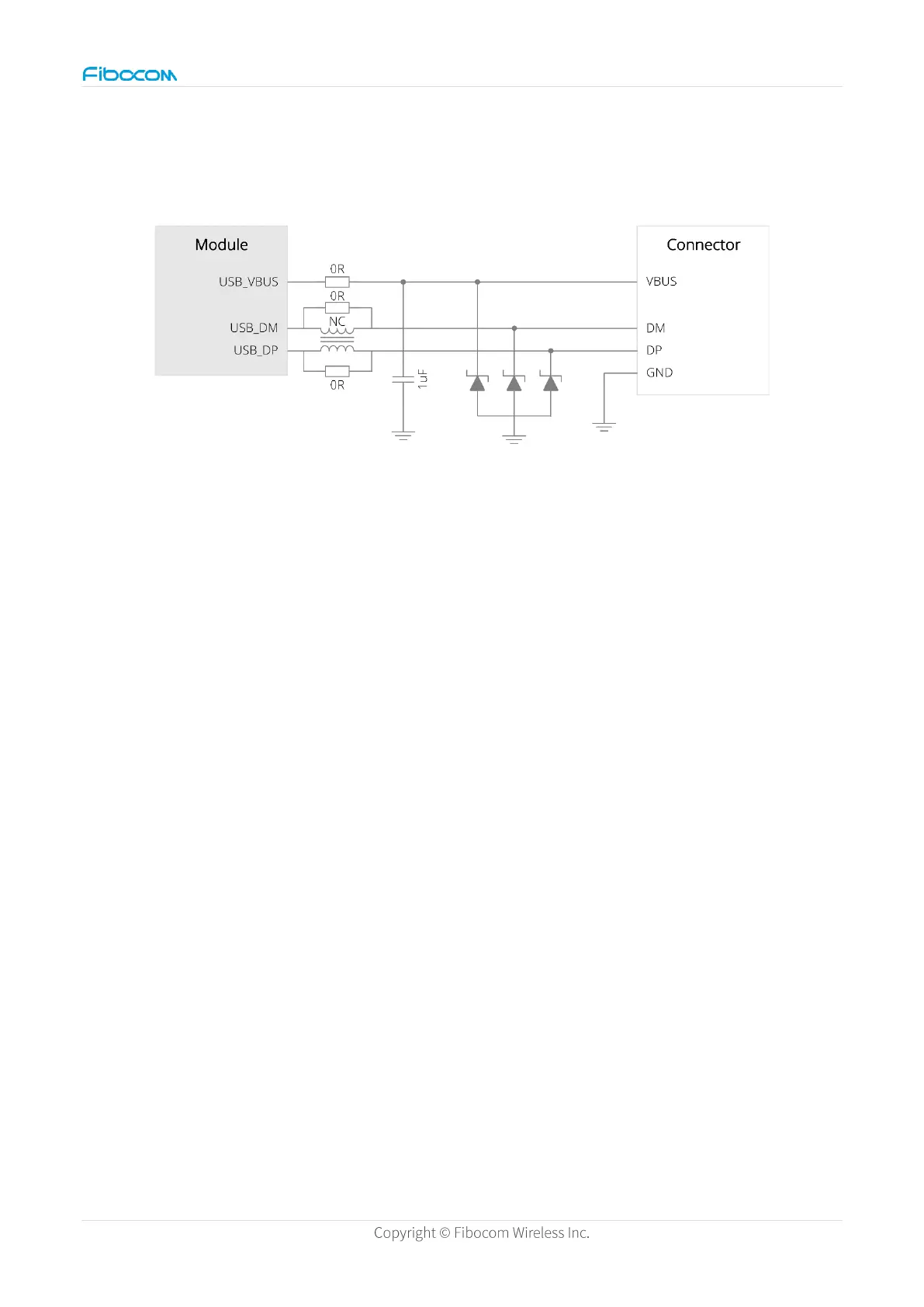
Schematic Diagram Design
The interface circuit design is shown in the following figure.
Figure 13. Interface circuit design
Since the module supports USB 2.0 High-Speed, it is recommended to use TVS with a
capacitance of 0.5 pF on the USB_DM/DP differential signal line. It is recommended to
connect a 0-ohm resistor on each USB_DM/DP differential line to facilitate debugging. USB
enumeration requires an additional voltage to USB_VBUS. Otherwise, USB cannot be
enumerated normally. The voltage range is 3.5V to 5.5V.
PCB Design
USB_DP and USB_DM are high-speed differential signal lines that should be equal in length
and parallel to avoid right-angle route. The difference of cabling length is controlled within ≤
2 mm, and the differential impedance is controlled at 90Ω±15%.
The USB data cable cannot be routed under the crystal, oscillator, magnetic device, or RF
signal. It is recommended to take an inner differential cable that is wrapped with copper
connected to the ground at all directions.
The ESD protector for the USB data cable must be placed close to the USB interface. The
parasitic capacitance of the ESD protector must not exceed 1 pF, and a TVS with a
capacitance of 0.5pF is recommended.
USB 2.0 differential signal cable should be laid on the signal layer nearest to the ground.
 Loading...