4 RF Interface
56
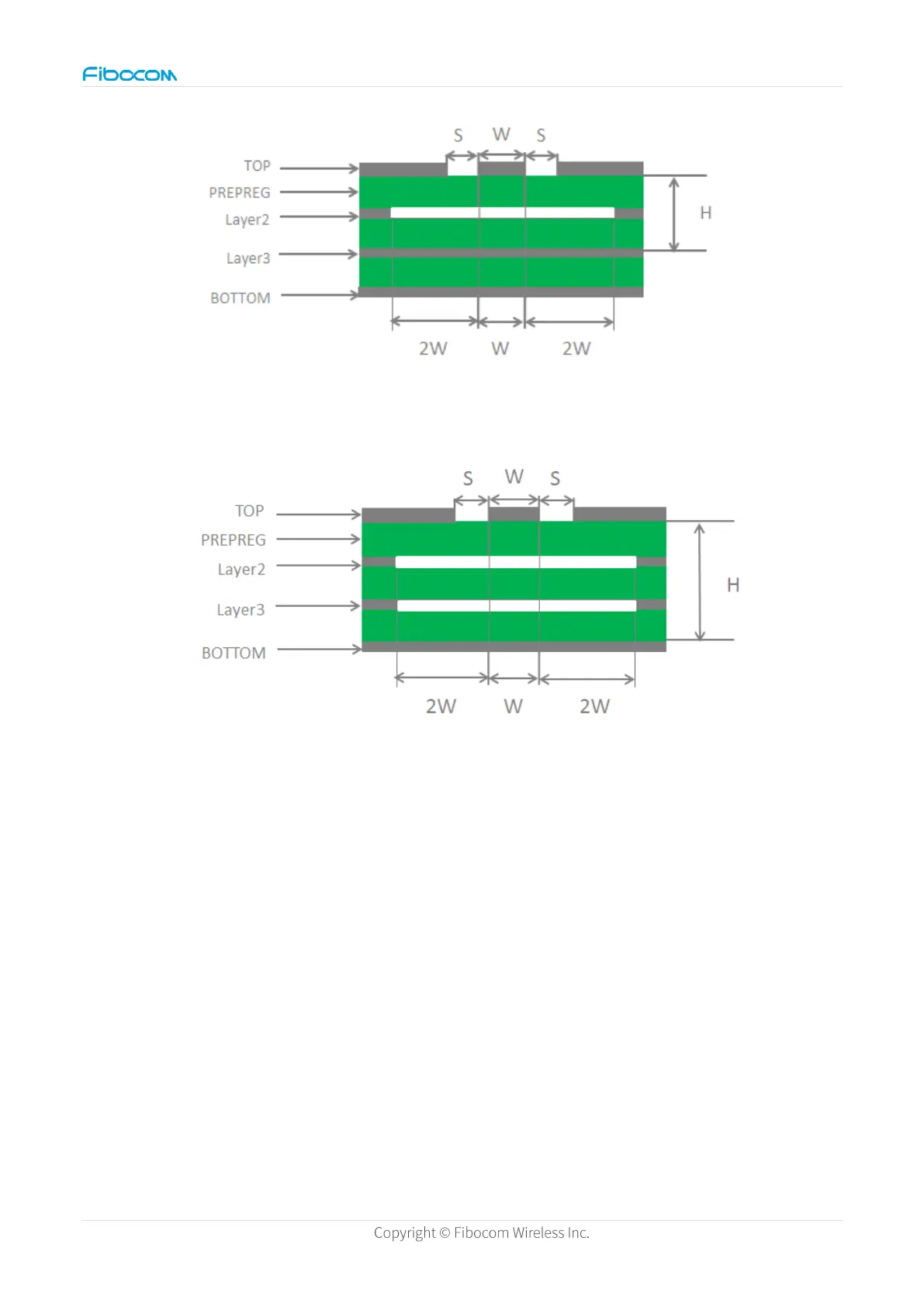
Figure 23. Four-layer PCB coplanar waveguide structure (see ground layer 3)
Figure 24. Four-layer PCB coplanar waveguide structure (see ground layer 4)
In the design of RF antenna interface circuit, in order to ensure good performance and
reliability of the RF signal, it is recommended to observe the following principles:
⚫ The impedance simulation tool should be used to accurately control the RF signal cable at
50Ω impedance.
⚫ The GND pin adjacent to the RF pin should not have thermal welding plate and should be
in full contact with the ground.
⚫ The distance between the RF pin and the RF connector should be as short as possible. At
the same time, avoid the right-angle route. The recommended route angle is 135°.
⚫ Attention should be paid to the establishment of the connection component package and
 Loading...