3-7
3.5 Communication Unit (IC-212)
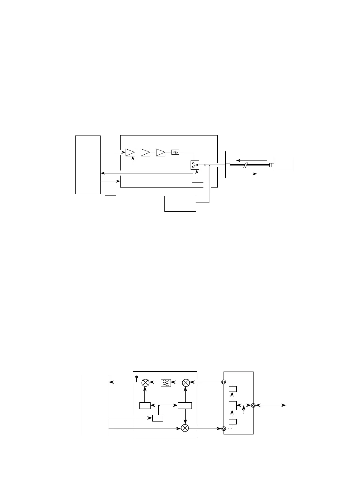
1. TX board (16P0157)
The TX board includes amplifier circuits and a transmission/reception switching
circuit. The receiving signal from the Antenna Unit is supplied to the RF CON board
through the transmission/reception switching circuit in the TX board. The switching
loss of the receiving signal is less than 2 dB.
The transmitting signal from RF CON board is amplified 28 dB and supplied to the
Antenna Unit through the transmission/reception switching circuit in the TX board.
RX: 1530 ~ 1545MHz
TX: 1626.5 ~ 1646.5MHz
TX (16P0157)
CR1
HSMP-3894
U1
µ
PC2709
Q1 Q2
AT42086 AT42086
FL1
DFC31R64P034BHA
C23
RX18V TX29V
ANT
TX +8 ~ 13dBm
RX -120.5 ~ -94.5dBm
TX RF
REG
(16P0149)
RF CON
(16P0147)
•
+12V
•
+5V TX ON
•
HPA ON
•
HPA ON
RX RF
+5V TX ON
•
HPA ON
•
HPA ON
Ant.unit
(IC-112)
Figure 3-5 Block Diagram of TX Board
2. RF CON board (16P0147)
A simplified block diagram of RF CON board is shown below. The RF CON board
includes a 15.6 MHz reference oscillator, a PLL synthesizer local oscillator for
transmission and reception, a BPSK transmitting modulator, and receiver circuits.
In the transmitting circuit a carrier of 1626.5 to 1646.5 MHz is modulated in BPSK by
serial data (S-DATA) which is supplied from CPU board.
In the receiving circuit a receiving signal of 1530.0 to 1545.0 MHz is converted to a
first IF signal of 90.05 MHz by mixing with a RX 1Lo signal of 1620.05 to 1635.05
MHz, and further converted to a second IF signal of 50 kHz by mixing with a RX 2Lo
signal of 90.1 MHz. This 50kHz signal (TP2: 4Vp-p) is supplied to the CPU board
and demodulated in BPSK there.
Block diagram of RF CON board is shown on next page.
TX
(16P0157)
CPU
(16P0148)
RF CON (16P0147)
PLL3 PLL1/2
1620.05 ~
1635.05MHz
1626.5 ~
1646.5MHz
90.05MHz
90.1MHz
50kHz
S-DATA
RX: 1530 ~
1545MHz
TX: 1626.5 ~
1646.5MHz
REF
REF CONT
15.6MHz
SW
RX18V
T/RX Vcc
T/RX L Band
TX 29V
BPSK MOD
TP2
(4Vp-p)
Figure 3-6 Block Diagram of RF CON Board
 Loading...