3-9
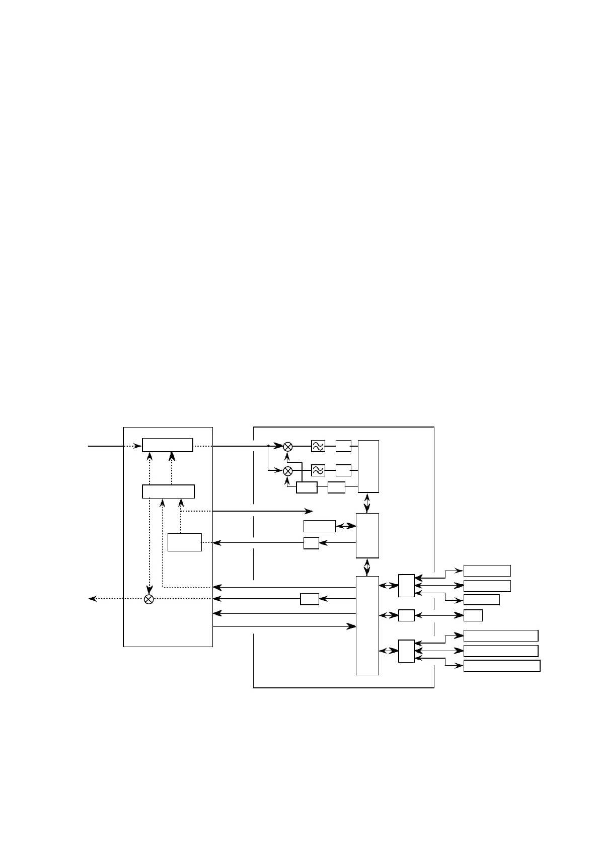
3. CPU board (16P0148)
A simplified block diagram of the CPU board is shown below. The CPU board
includes CPU1, CPU2, and interfacing circuits with outside. The functions of CPU1
are BPSK demodulation, and receiving signal processing, such as unique word
detection, de-permutation, de-interleaving, Viterbi decoding, de-scrambling, and
packet separation. The functions of CPU2 are communication protocol control, system
control for operating units, communication with terminal units, and processing of
transmitting data signal, such as scrambling, convolution encoding, adding unique
words, interleaving, permutation, and adding preambles.
The receiving 50kHz signal from the RF CON board is demodulated in BPSK and
quantized to a 3-bit signal. That is, the demodulated output (H- or L-level) is
expressed by 3 bits to indicate which level, H or L, is more probable for the output.
For example, if all three bits are H, it means it is most probable for the signal to be H.
This 3-bit quantized signal is processed in CPU 1 and then passed to CPU2. In
accordance with the content of the signal, CPU2 delivers a message to the own ship
and EGC message to terminals, or follows a protocol of communicative information.
During transmission, transmitting data such as IA2, ITA5, and DATA (binary) from
terminal units input to CPU2 through interfaces. CPU2 processes the transmitting
signal and outputs serial data (S-DATA) to RF CON board, where the serial data is
modulated in BPSK.
A/D
A/D
DSP
DDS
0/90
°
D/A
SHR
I/F
CPU 1
CPU 2
VITERBI
I/F
DTE 1 : IB-581
DTE 2 : IB-581
PC/DATA
NAV
Distress alert unit : IC-302
Received call unit : IC-303
Distress alert unit : IC-302
I/F
REF CONT
S-DATA (TX)
CPU
(16P0148)
3 bit digital data
Signal
processing
1) RX Signal processing
2) TX Signal prosessimg
3) Communication protocol controlling
4) System Contorolling
5) Interfacing
SYN DATA
System control data (TX ON,HPA ON)
Detected data (PLL, AGC LVL)
BPSK modulation
RX: 50kHz
RF CON
(16P0147)
PLL 1/2/3
REF
(15.6MHz)
Receiver
BPSK modulation
15.6MHz T/RX REF CLK
1.5GHz
1.6GHz
Figure 3-8 Block Diagram of RF CON and CPU Boards
 Loading...