M24Cxx-W, M24Cxx-R, M24Cxx-F Signal description
9/34
2.3 Supply voltage (V
CC
)
2.3.1 Operating supply voltage V
CC
Prior to selecting the memory and issuing instructions to it, a valid and stable V
CC
voltage
within the specified [V
CC
(min), V
CC
(max)] range must be applied (see Table 8 and Ta bl e 9 ).
In order to secure a stable DC supply voltage, it is recommended to decouple the V
CC
line
with a suitable capacitor (usually of the order of 10nF to 100nF) close to the V
CC
/V
SS
package pins.
This voltage must remain stable and valid until the end of the transmission of the instruction
and, for a Write instruction, until the completion of the internal write cycle (t
W
).
2.3.2 Internal device reset
In order to prevent inadvertent Write operations during Power-up, a Power On Reset (POR)
circuit is included. At Power-up (continuous rise of V
CC
), the device does not respond to any
instruction until V
CC
has reached the Power On Reset threshold voltage (this threshold is
lower than the minimum V
CC
operating voltage defined in Table 8 and Tabl e 9).
When V
CC
has passed the POR threshold, the device is reset and is in Standby Power
mode.
2.3.3 Power-down
At Power-down (continuous decrease of V
CC
), as soon as V
CC
drops from the normal
operating voltage to below the Power On Reset threshold voltage, the device stops
responding to any instruction sent to it.
During Power-down, the device must be deselected and in the Standby Power mode (that is
there should be no internal Write cycle in progress).
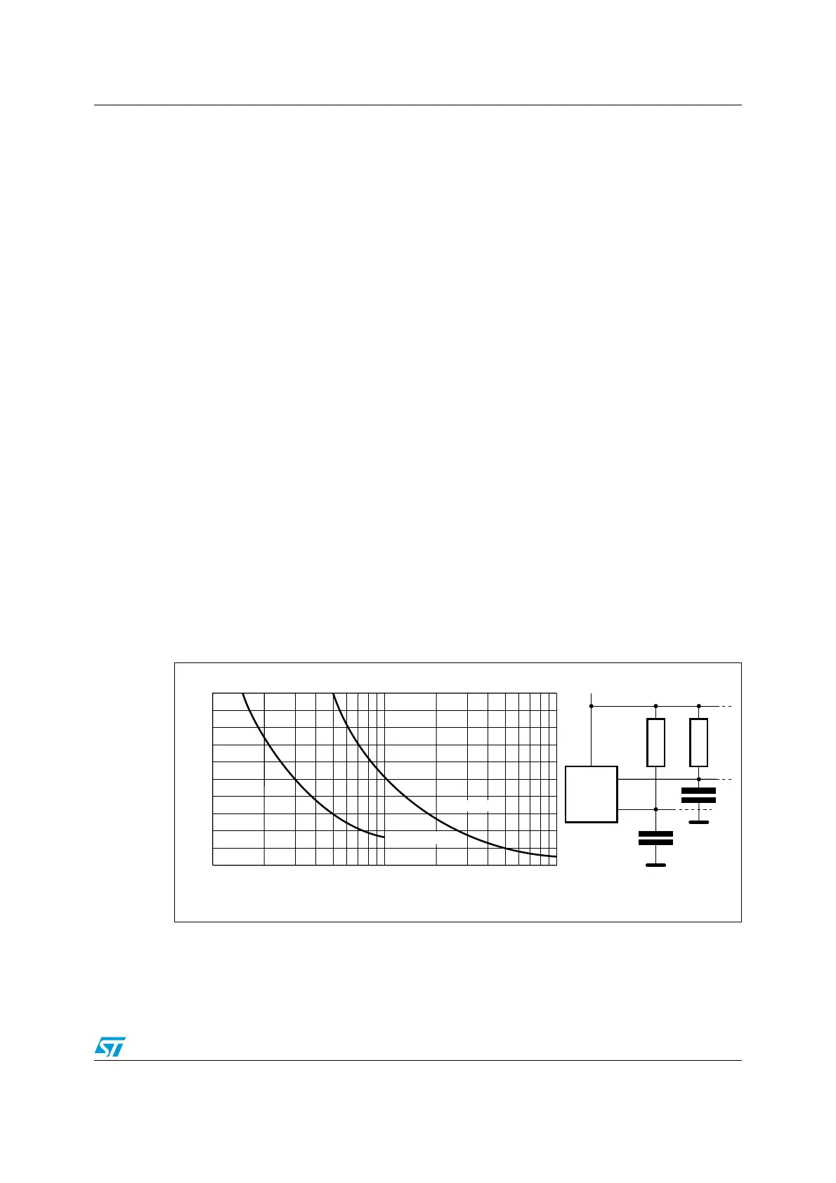
Figure 4. Maximum R
P
value versus bus parasitic capacitance (C) for an I
2
C bus
AI01665b
V
CC
C
SDA
R
P
MASTER
R
P
SCL
C
100
0
4
8
12
16
20
C (pF)
Maximum RP value (kΩ)
10 1000
fc = 400kHz
fc = 100kHz
Harman Kardon
VR 151 Service Manual
Page 103 of 131
 Loading...