2
P/N: PM1237
REV. 2.2, OCT. 23, 2008
MX25L8005
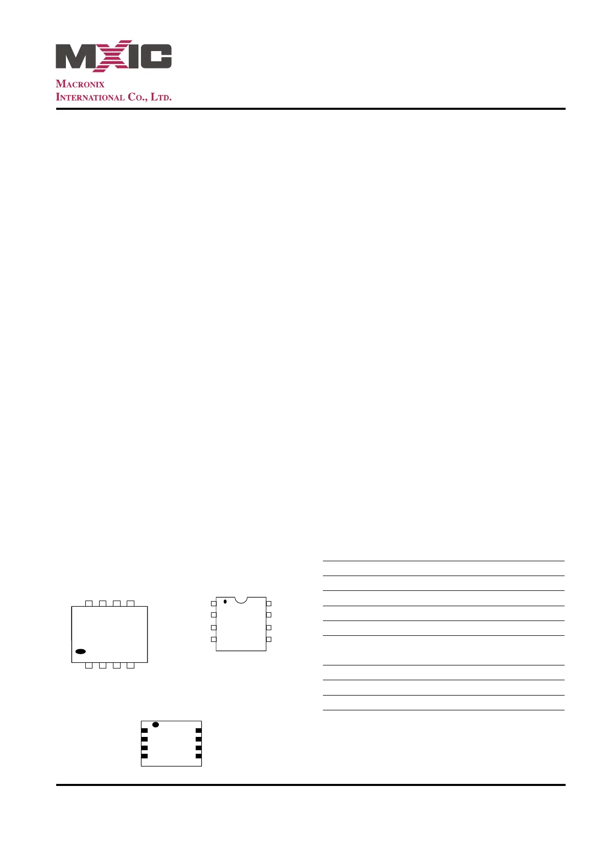
PIN CONFIGURATIONS
SYMBOL DESCRIPTION
CS# Chip Select
SI Serial Data Input
SO Serial Data Output
SCLK Clock Input
HOLD# Hold, to pause the device without
deselecting the device
WP# Write Protection
VCC + 3.3V Power Supply
GND Ground
PIN DESCRIPTION
GENERAL DESCRIPTION
The MX25L8005 is a CMOS 8,388,608 bit serial Flash memory, which is configured as 1,048,576 x 8 internally. The
MX25L8005 feature a serial peripheral interface and software protocol allowing operation on a simple 3-wire bus. The three
bus signals are a clock input (SCLK), a serial data input (SI), and a serial data output (SO). SPI access to the device is
enabled by CS# input.
The MX25L8005 provide sequential read operation on whole chip.
After program/erase command is issued, auto program/ erase algorithms which program/ erase and verify the specified
page or byte /sector/block locations will be executed. Program command is executed on page (256 bytes) basis, and erase
command is executes on chip or sector(4K-bytes) or block(64K-bytes).
To provide user with ease of interface, a status register is included to indicate the status of the chip. The status read
command can be issued to detect completion status of a program or erase operation via WIP bit.
When the device is not in operation and CS# is high, it is put in standby mode and draws less than 10uA DC current.
The MX25L8005 utilize MXIC's proprietary memory cell, which reliably stores memory contents even after 100,000 program
and erase cycles.
8-PIN SOP (150/200mil)
* 8-LAND SON/WSON (6x5mm), USON (4x4mm)
1
2
3
4
CS#
SO
WP#
GND
8
7
6
5
VCC
HOLD#
SCLK
SI
1
2
3
4
CS#
SO
WP#
GND
VCC
HOLD#
SCLK
SI
8
7
6
5
8-PIN PDIP (300mil)
• WP# pin
- Hardware write protection
• HOLD# pin
- pause the chip without diselecting the chip
• PACKAGE
- 8-pin SOP (150mil)
- 8-pin SOP (200mil)
- 8-pin PDIP (300mil)
- 8-land SON/WSON (6x5mm), 8-land SON is not recommended for new design
- 8-land USON (4x4mm)
- All Pb-free devices are RoHS Compliant
1
2
3
4
CS#
SO
WP#
GND
8
7
6
5
VCC
HOLD#
SCLK
SI
Note: 8-land SON is not recommended for new design
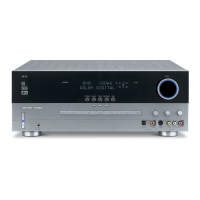
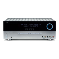
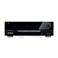
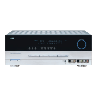
Harman Kardon
VR 151 Service Manual
Page 93 of 131
 Loading...