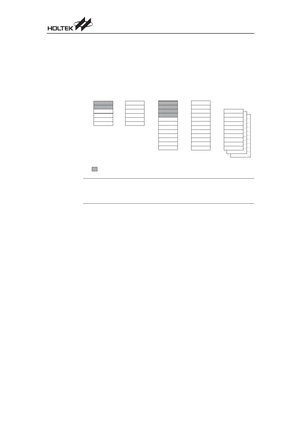
HT48RU80/HT48CU80 devices, known as Bank 0, Bank 1 and Bank 2, it is necessary to first en
-
sure that the Bank Pointer is properly set to the correct value before accessing the General Pur
-
pose Data Memory. Bank 1 or Bank 2 must be addressed indirectly using the Memory Pointer MP1
and the indirect addressing register IAR1. Any direct addressing or any indirect addressing using
MP0 and IAR0 will always result in data from Bank 0 being accessed.
The following diagram shows the General Purpose Data Memory Organization Map for the I/O
Type microcontrollers:
Note
The 576 bytes of the General Purpose Data Memory in the HT48RU80/HT48CU80 devices are
stored in three individual memory banks, known as Bank 0, Bank 1 and Bank 2. Before reading or
writing to the General Purpose Data Memory it is essential to first ensure that the correct Data
Memory bank is selected by setting up the Bank Pointer.
Chapter 1 Hardware Structure
29
H T 4 8 R 7 0 A - 1
H T 4 8 C 7 0 - 1
F F H
2 0 H
2 2 4 B y t e s
H T 4 8 R 5 0 A - 1
H T 4 8 C 5 0 - 1
F F H
2 0 H
6 0 H
1 6 0 B y t e s
H T 4 8 R 3 0 A - 1
H T 4 8 C 3 0 - 1
2 0 H
9 6 B y t e s
H T 4 8 R 1 0 A - 1
H T 4 8 C 1 0 - 1
7 F H
2 0 H
6 4 B y t e s
H T 4 8 R U 8 0
H T 4 8 C U 8 0
F F H
B a n k 0
4 0 H
B a n k 1
5 7 6 B y t e s
B a n k 2
4 0 H
7 F H
: U n u s e d , R e a d a s " 0 0 "