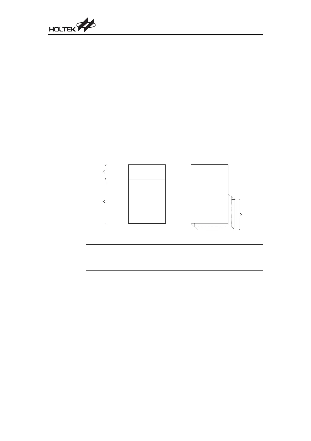
Data Memory
The Data Memory is a volatile area of 8-bit wide RAM internal memory and is the location where
temporary information is stored. Divided into two sections, the first of these is an area of RAM
where special function registers are located. These registers have fixed locations and are neces
-
sary for correct operation of the device. Many of these registers can be read from and written to di
-
rectly under program control, however, some remain protected from user manipulation. The
second area of Data Memory is reserved for general purpose use. All locations within this area are
read and write accessible under program control. For the HT48RU80/HT48CU80 devices, this
General Purpose Data Memory is divided into three banks, Bank 0, Bank 1 and Bank 2.
Organization
The two sections of Data Memory, the Special Purpose and General Purpose Data Memory are lo
-
cated at consecutive locations. All are implemented in RAM and are 8 bits wide but the length of
each memory section is dictated by the type of microcontroller chosen. The start address of the
Data Memory for all devices is the address 00H. The last Data Memory address is 7FH for the
HT48R10A-1/HT48C10-1 and HT48R30A-1/HT48C30-1 devices, and FFH for the HT48R50A-1/
HT48C50-1, HT48R70A-1/HT48C70-1 and HT48RU80/HT48CU80 devices. Registers which are
common to all microcontrollers, such as ACC, PCL, etc., have the same Data Memory address.
Note
Most of the Data Memory bits can be directly manipulated using the ²SET [m].i² and ²CLR [m].i²
with the exception of a few dedicated bits. The Data Memory can also be accessed through the
Memory Pointer register MP for the HT48R10A-1/HT48C10-1 and HT48R30A-1/HT48C30-1. For
the other devices there are two Memory Pointer registers MP0 and MP1.
General Purpose Data Memory
All microcontroller programs require an area of read/write memory where temporary data can be
stored and retrieved for use later. It is this area of RAM memory that is known as General Purpose
Data Memory. This area of Data Memory is fully accessible by the user program for both read and
write operations. By using the ²SET [m].i² and ²CLR [m].i² instructions individual bits can be set or
reset under program control giving the user a large range of flexibility for bit manipulation in the
Data Memory. As the General Purpose Data Memory exists in three separate Banks for the
28
I/O Type MCU
S p e c i a l
P u r p o s e
D a t a
M e m o r y
0 0 H
2 0 H / 4 0 H / 6 0 H
7 F H / F F H
1 F H / 3 F H / 5 F H
B a n k 0
G e n e r a l
P u r p o s e
D a t a
M e m o r y
C a p a c i t y
i s D e v i c e
D e p e n d e n t
B a n k 0 , 1 , 2
G e n e r a l
P u r p o s e
D a t a
M e m o r y
B a n k 0
B a n k 1
B a n k 2
H T 4 8 R 1 0 A - 1 / H T 4 8 C 1 0 - 1 , H T 4 8 R 3 0 A - 1 / H T 4 8 C 3 0 - 1
H T 4 8 R 5 0 A - 1 / H T 4 8 C 5 0 - 1 , H T 4 8 R 7 0 A - 1 / H T 4 8 C 7 0 - 1
H T 4 8 R U 8 0 / H T 4 8 C U 8 0
3 F H
4 0 H
F F H
0 0 H