Programmable Frequency Divider (PFD) and Buzzer Application
Operating similar to a programmable frequency divider, the buzzer function within the
microcontroller provides a means of producing a variable frequency output suitable for applica
-
tions such as piezo-buzzer driving or other interfaces requiring a precise frequency generator.
The BZ and BZ
are a complimentary pair and pin-shared with I/O pins, PB0 and PB1. The function
is selected via configuration option to have single BZ output or both BZ and BZ
outputs, however, if
not selected, the pins can operate as normal I/O pins. Note that the BZ
pin is the inverse of the BZ
pin generating a kind of differential output and supplying more power to connected interfaces such
as buzzers.
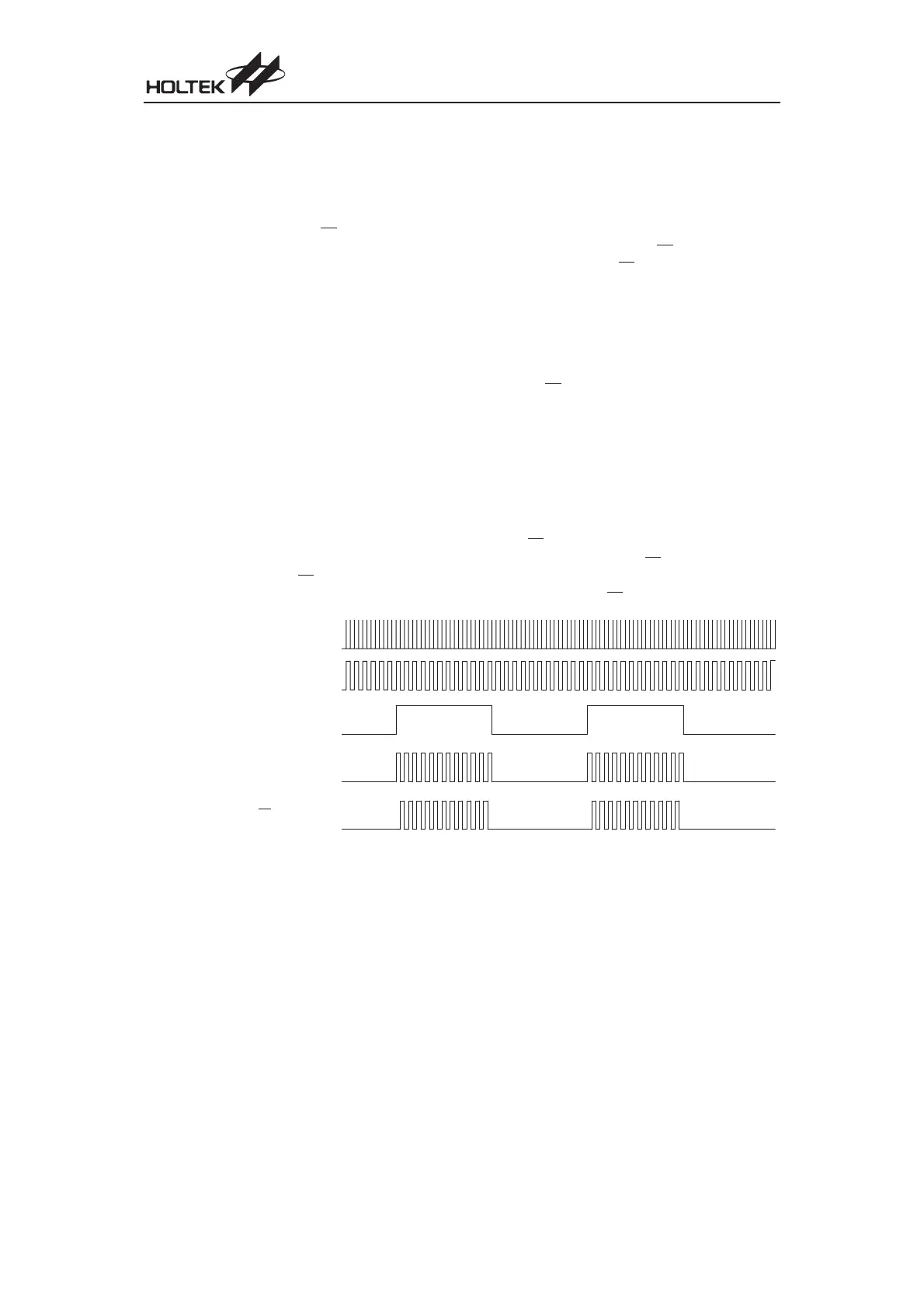
The timer overflow signal is the clock source for the buzzer circuit. The output frequency is con
-
trolled by loading the required values into the timer prescaler registers to give the required division
ratio. The counter will begin to count-up from this preload register value until full, at which point an
overflow signal is generated, causing both the BZ and BZ
outputs to change state. The counter will
then be automatically reloaded with the preload register value and continue counting-up. Refer to
the relevant Timer/Event Counters section for details of its settings and operations. For the
HT48R50A-1/HT48C50-1 and HT48RU80/HT48CU80 devices, either Timer/Event Counter 0 or
Timer/Event Counter 1 can form the clock source for the Buzzer function. For the HT48R70A-1/
HT48C70-1 devices, only Timer/Event Counter 0 can form the Buzzer clock source.
For the buzzer outputs to function, it is essential that the Port B control register PBC bit 0 and PBC
bit 1 are setup as outputs. If they are setup as inputs the buzzer output will not function, and the
pins can be used as normal input pins. The BZ and BZ
outputs will only be activated if bit PB0 is set
to ²1². This output data bit is used as the on/off control bit for the BZ and BZ
outputs. Note that the
BZ and BZ
outputs will both be low if the PB0 output data bit is cleared to ²0². Note that the condi-
tion of bit PB1 has no effect on the overall control of the BZ and BZ
pins.
Using this method of frequency generation, and if a crystal oscillator is used for the system clock,
very precise values of frequency can be generated.
Chapter 1 Hardware Structure
49
T i m e r O v e r f l o w
B u z z e r C l o c k
P B 0 D a t a
B Z O u t p u t a t P B 0
B Z O u t p u t a t P B 1
PFD Output Control