'
SERIES
UN
R
EG ULATEO
RECTIFIERS
Dc
FROM
"OLTAGE-
REGULATOR
DIFFER
ENTI
A
L
AMPLIFIER
REGULATED
DC OUTPUT
I
-+
REFERENCE
VOLTAGE
141.-1-1
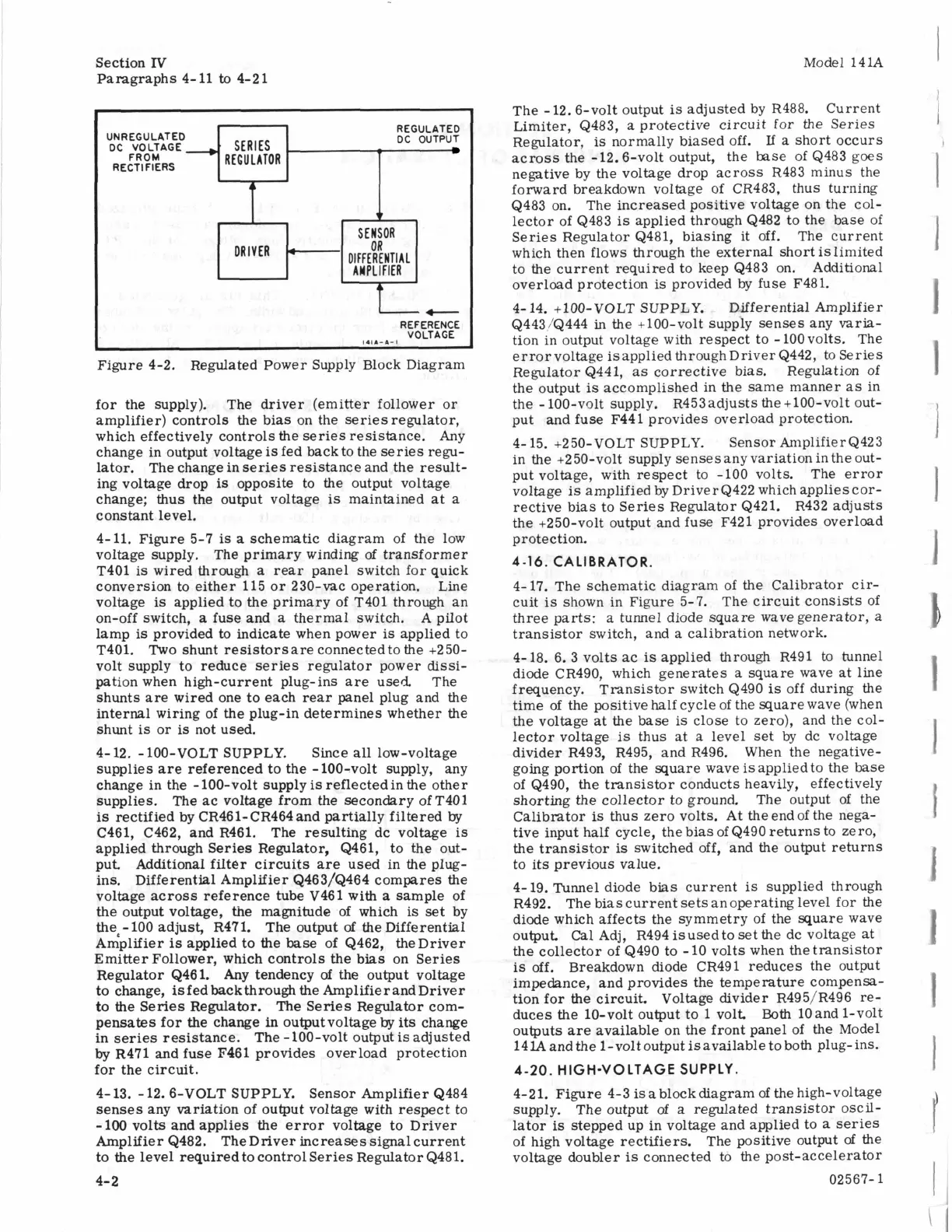
Figure 4-2.
Regulated Power Supply Block Diagram
for the supply). The driver (emitter follower
or
amplifier) controls
the
bias on the series regulator,
which effectively controls the series resistance. Any
change in output voltage is fed back to the series regu-
lator. The change
in
series resistance and the result-
ing voltage drop
is
opposite to the output voltage
change; thus the output voltage
is
maintained at
a
constant level.
4-11. Figure 5-7
is
a
schematic diagram of the low
voltage supply. The primary winding of transformer
T401 is wired through
a
rear panel switch for quick
conversion to either 115 or 230-vac operation.
Line
voltage
is
applied to the primary of T401 through an
on-off switch,
a
fuse and
a
thermal switch.
A
pilot
lamp
is
provided to indicate when power
is
applied to
T401.
Two
shunt resistorsare connectedto the +250-
volt supply to reduce series regulator power dissi-
pation when high-current plug-ins
are
used
shunts are wired one to each
rear
panel plug and the
internal wiring of the plug-in determines whether the
shunt
is
or
is
not used.
4- 12. -100-VOLT SUPPLY.
supplies
are
referenced to the
-
100-volt supply, any
change in the -100-volt supply
is
reflectedin the other
supplies. The ac voltage from the secondary of T401
is
rectified by CR461-CR464 and partially filtered
by
C461, C462, and R461.
The resulting dc voltage
is
applied through Series Regulator, Q461, to the out-
put. Additional
filter
circuits are used in the plug-
ins. Differential Amplifier Q463/Q464 compares the
voltage across reference tube V461 with
a
sample of
the output voltage, the magnitude of which
is
set
by
theo- 100 adjust, R471. The output
of
the Differential
Amplifier
is
applied to the
base
of Q462,
theDriver
Emitter Follower, which controls the bias on Series
Regulator Q461.
Any
tendency
of
the output voltage
to change,
is
fedbackthrough the AmplifierandDriver
to
the
Series Regulator.
The Series Regulator com-
pensates for the change
in
outputvoltage
by
its
change
in series resistance. The -100-volt output
is
adjusted
by
R471
and
fuse F461 provides overload protection
for the circuit.
4-
13.
-
12.6-VOLT SUPPLY.
Sensor Amplifier Q484
senses any variation of output voltage with respect to
-100 volts and applies the error voltage to Driver
Amplifier Q482. TheDriver increases signalcurrent
to
the
level required to control Series Regulator Q481.
The
Since
all
low-voltage
4-
2
Model 141A
The -12.6-volt output
is
adjusted by R488. Current
Limiter, Q483,
a
protective circuit for the Series
Regulator,
is
normally biased off.
If
a
short occurs
across the -12.6-volt output, the base of Q483 goes
negative by the voltage drop across R483 minus the
forward breakdown voltage
of
CR483, thus turning
Q483 on. The increased positive voltage on the col-
lector of Q483
is
applied through Q482 to the base of
Series Regulator Q481, biasing it off. The current
which then flows through the external short
is
limited
to the current required to keep Q483 on.
Additional
overload protection is provided
by
fuse F481.
4-
14.
+100-VOLT SUPPLY. Differential Amplifier
Q443/Q444
in
the +lOO-volt supply senses any varia-
tion in output voltage with respect to
-
100 volts. The
errorvoltage isapplied throughDriver Q442, to Series
Regulator Q441,
as
corrective bias. Regulation of
the output
is
accomplished in the same manner
as
in
the
-
100-volt supply. R453adjusts the +lOO-volt out-
put and fuse F441 provides overload protection.
4- 15. +250-VOLT SUPPLY. Sensor AmplifierQ423
in
the
+2
50-volt supply sensesanyvariation in the out-
put voltage, with respect to -100 volts.
The error
voltage is amplified by DriverQ422 which applies cor-
rective bias to Series Regulator Q421. R432 adjusts
the +250-volt output and fuse
F421
provides overload
protection.
4-1
6.
CALI BRAT0
R.
4-17. The schematic diagram of the Calibrator cir-
cuit is shown in Figure
5-7.
The circuit consists of
three parts:
a
tunnel diode square wave generator,
a
transistor switch, and
a
calibration network.
4-18. 6. 3 volts ac
is
applied through R491 to tunnel
diode CR490, which generates
a
square wave at line
frequency. Transistor switch Q490
is
off during the
time of the positive
half
cycle of the square wave (when
the voltage
at
the base is close to zero), and the col-
lector voltage
is
thus at
a
level set
by
dc voltage
divider R493, R495, and R496. When the negative-
going portion of the square wave
is
appliedto the base
of Q490, the transistor conducts heavily, effectively
shorting the collector to ground. The output
of
the
Calibrator
is
thus zero volts. At theendof the nega-
tive input half cycle, the bias of Q490 returns to zero,
the transistor
is
switched off, and the output returns
to its previous value.
4-19. Tunnel diode bias current
is
supplied through
R492. The bias current
sets
anoperating level for the
diode which affects the symmetry of the square wave
output.
Cal
Adj, R494 isusedto set the dc voltage at
the collector
of
Q490 to
-
10 volts when the transistor
is
off. Breakdown diode CR491 reduces the output
impedance, and provides the temperature compensa-
tion for
the
circuit. Voltage divider R495/R496 re-
duces the 10-volt output to
1
volt. Both lOand 1-volt
outputs
are
available on the front panel of the Model
14lAandthe 1-voltoutput isavailable to both plug-ins.
4-20.
HIGH-VOLTAGE SUPPLY.
4-21.
Figure
4-3
is
ablockdiagram of the high-voltage
supply. The output
of
a
regulated transistor oscil-
lator
is
stepped up in voltage and applied to
a
series
of high voltage rectifiers. The positive output
of
the
voltage doubler
is
connected to the post-accelerator
02567-
1