Evaluation Board
User’s Manual 12 Rev. 1.2, 2013-06-06
Software Description for Evaluation Kits
3.1 Hardware Settings of the Evaluation Board
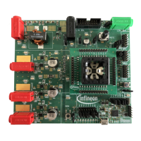
The Evaluation Board allows the operation of the TLI4970 current sensor under different test conditions. This
chapter describes the different jumper settings, which can be used for the evaluation of the TLI4970 current
sensor. The locations of the different jumpers are marked in Figure 8.
Note: The level shifter ICs (IC1 and IC2) on the Evaluation Board are only needed since the micro controller of the
PGSISI-2 is operated on +5 V, while the TLI4970 is operated with a supply voltage of +3.3 V. In order to
allow reliable communication between the two voltage domains, the level shifter ICs are needed.
3.1.1 Mounting Options for the Current Sensor
The Evaluation Board has two mounting options for the TLI4970 current sensor. It can be placed inside a socket
or can directly be soldered onto the PCB. Please note that at any time only one sensor can be operated. Therefore,
when operating the soldered sensor (DUT), the socket (DUT_SOCKET) needs to be empty. On the other hand, if
the sensor in the socket (DUT_SOCKET) is used, the soldered current sensor (DUT) or the 0 Ohm resistors (R16
- R19, see Figure 8) must be removed. Due to overloading of the pogo-pins of the socket, please do not
apply more than 10 A to the Evaluation Board, if a current sensor is located inside the socket
(DUT_SOCKET). If current sensor is soldered onto the PCB and the socket is empty, the board can be loaded
with a maximum of 50 A
peak
.
3.1.2 Normal Operation
During normal operation the full functionality of the TLI4970 can be tested without the need for any external power
supplies or connections. All needed voltages for the sensor and the level shifter ICs are supplied by the PGSISI-
2. All jumpers need to be in their default setting as specified in Table 3 and shown in Figure 9.
The current to be measured can be applied via two standard 4mm “Banana” plugs or by the two screw lugs with
7mm screw bolts. For maximum current loading of the socket and the board please refer to Table 2.
The operation of the SPI interface can be monitored via the connectors JP1. This also allows the connection of a
logic analyzer. The overcurrent response of the TLI4970 can be monitored via the OCD-pin. This pin also allows
monitoring of the SICI
1)
-interface, which is used for EEPROM programming.
1) SICI: Serial Inspection and Configuration Interface (Infineon proprietary interface and protocol)
Table 3 Default jumper settings
Name Label Default setting Comment
J4 Vprog Closed Enables programming voltage on CS
pin for EEPROM
programming
J8 CS_B Closed Enabling of SPI communication to sensor
J10 DIN_OCD Open Data-Input for 4-pin SPI communication
1)
1) Needs to be enabled via EEPROM programming. Currently not available.
JP4 GND GND-PGSISI Allows disconnection of sensor GND from PGSISI-2
JP6 V3V3 V3V3-PGSISI Supply voltage V
DD
for sensor from PGSISI-2
 Loading...