8XC251SA, SB, SP, SQ USER’S MANUAL
7-4
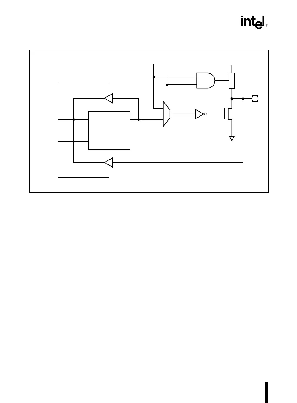
Figure 7-3. Port 2 Structure
When port 0 and port 2 are used for an external memory cycle, an internal control signal switches
the output-driver input from the latch output to the internal address/data line. Section 7.8, “Exter-
nal Memory Access,” discusses the operation of port 0 and port 2 as the external address/data bus.
NOTE
Port 0 and port 2 are precluded from use as general purpose I/O ports when
used as address/data bus drivers.
Port 0 internal pullups assist the logic-one output for memory bus cycles only.
Except for these bus cycles, the pullup FET is off. All other port 0 outputs are
open drain.
Read
Latch
Read
Pin
Address
Control
D
CL
Q
Q#
P2.
x
Latch
V
CC
Internal
Pullup
A2240-01
P2.
x
Write to
Latch
Internal
Bus
1
0