8XC251SA, SB, SP, SQ USER’S MANUAL
13-18
13.8 EXTERNAL MEMORY DESIGN EXAMPLES
This section presents several external memory designs for 8XC251Sx systems. These examples
illustrate the design flexibility provided by the configuration options, especially for the PSEN#
and RD# signals. Many designs are possible. The examples employ the 8XC251SB but also apply
to SA, SP, and SQ devices if the differences in on-chip memory are allowed for. The first example
is an exception; it employs an 18-bit external address bus. For a general discussion on external
memory see “Configuring the External Memory Interface” on page 4-8. Figure 4-5 on page 4-10
and Figure 4-6 on page 4-11 depict the mapping of internal memory space into external memory.
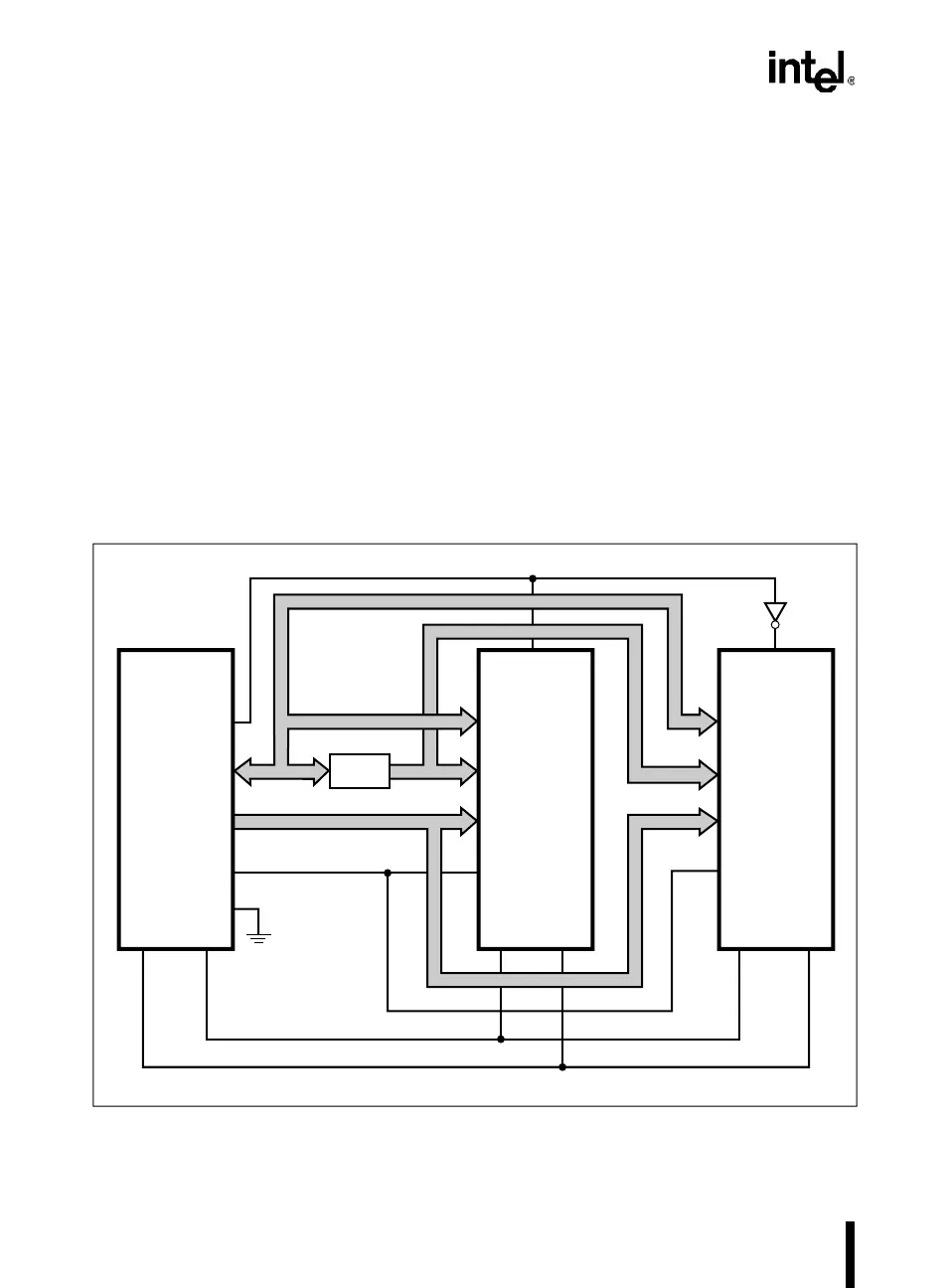
13.8.1 Example 1: RD1:0 = 00, 18-bit Bus, External Flash and RAM
In this example, an 80C251SB operates in page mode with an 18-bit external address bus inter-
faced to 128 Kbytes of external flash memory and 128 Kbytes of external RAM (Figure 13-17).
Figure 13-18 shows how the external flash and RAM are addressed in the internal address space.
On-chip data RAM (1056 bytes) occupies the lowest addresses in region 00:.
Figure 13-17. Bus Diagram for Example 1: 80C251SB in Page Mode
A4219-01
80C251SB
A17
P2
P0
A16
EA#
WR# PSEN#
CE#
D7:0
A15:8
A7:0
A16
OE# WE#
CE#
D7:0
A15:8
A7:0
A16
OE# WE#
RAM
(128 Kbytes)
Flash
(128 Kbytes)
Latch
i_extmem.fm5 Page 18 Thursday, June 27, 1996 1:40 PM