13-1
CHAPTER 13
EXTERNAL MEMORY INTERFACE
13.1 OVERVIEW
The external memory interface comprises the external bus (ports 0 and 2, and when enabled also
includes port 1.7:6) as well as the bus control signals (RD#, WR#, PSEN# and ALE). Chip con-
figuration bytes (see Chapter 4, “Device Configuration”) determine several interface options:
page mode or nonpage mode for external code fetches; the number of external address bits (16,
17, or 18); the address ranges for RD#, WR#, and PSEN#; and the number of preprogrammed
external wait states to extend RD#, WR#, PSEN# or ALE. Real-time wait states can be enabled
with special function register WCON.1:0. You can use these options to tailor the interface to your
application. See also section 4.5, “Configuring the External Memory Interface.”
The external memory interface operates in either page mode or nonpage mode. Page mode pro-
vides increased performance by reducing the time for external code fetches. Page mode does not
apply to code fetches from on-chip memory. The reset routine configures the 8XC251Sx for op-
eration in page mode or nonpage mode according to bit 1 of configuration byte UCONFIG0. Fig-
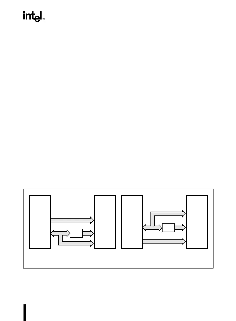
ure 13-1 shows the structure of the external address bus for page and nonpage mode operation.
P0 carries address A7:0 while P2 carries address A15:8. Data D7:0 is multiplexed with A7:0 on
P0 in nonpage mode and with A15:8 on P2 in page mode.
Table 13-1 describes the external memory interface signals. The address and data signals (AD7:0
on port 0 and A15:8 on port 2) are defined for nonpage mode.
Figure 13-1. Bus Structure in Nonpage Mode and Page Mode
A4159-02
D7:0
A15:8
A7:0
A15:8
P2
P0
A7:0
8XC251SA
8XC251SB
8XC251SP
8XC251SQ
RAM/
EPROM/
Flash
AD7:0
Latch
A7:0
D7:0
A15:8
A7:0
P2
P0
A15.8
8XC251SA
8XC251SB
8XC251SP
8XC251SQ
RAM/
EPROM/
Flash
A15:8/D7:0
Latch
Nonpage Mode Page Mode