8XC251SA, SB, SP, SQ USER’S MANUAL
13-30
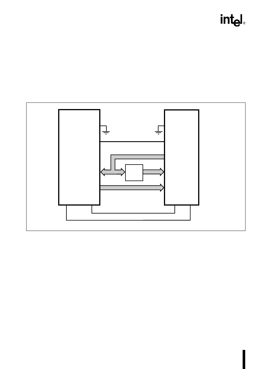
13.8.7 Example 7: RD1:0 = 01, 17-bit Bus, External Flash
In this example, an 80C251SB operates in page mode with a 17-bit external address bus inter-
faced to 128 Kbytes of flash memory (Figure 13-28). Port 2 carries both the upper address bits
(A15:0) and the data (D7:0), while port 0 carries only the lower address bits (A7:0). The
80C251SB is configured for a single read signal (PSEN#). The 128 Kbytes of external flash are
accessed via internal memory regions FE: and FF: in the internal address space.
Figure 13-28. Bus Diagram for Example 7: 80C251SB in Page Mode
PSEN#
80C251SB
A4151-01
WR#
FLASH
(128 Kbytes)
OE#
WE#
A15:8/D7:0
A15:8
P2
P0
A15:8
A7:0
A7:0
Latch
D7:0
A16
CE#
A16
EA#
A16
Code