8XC251SA, SB, SP, SQ USER’S MANUAL
4-10
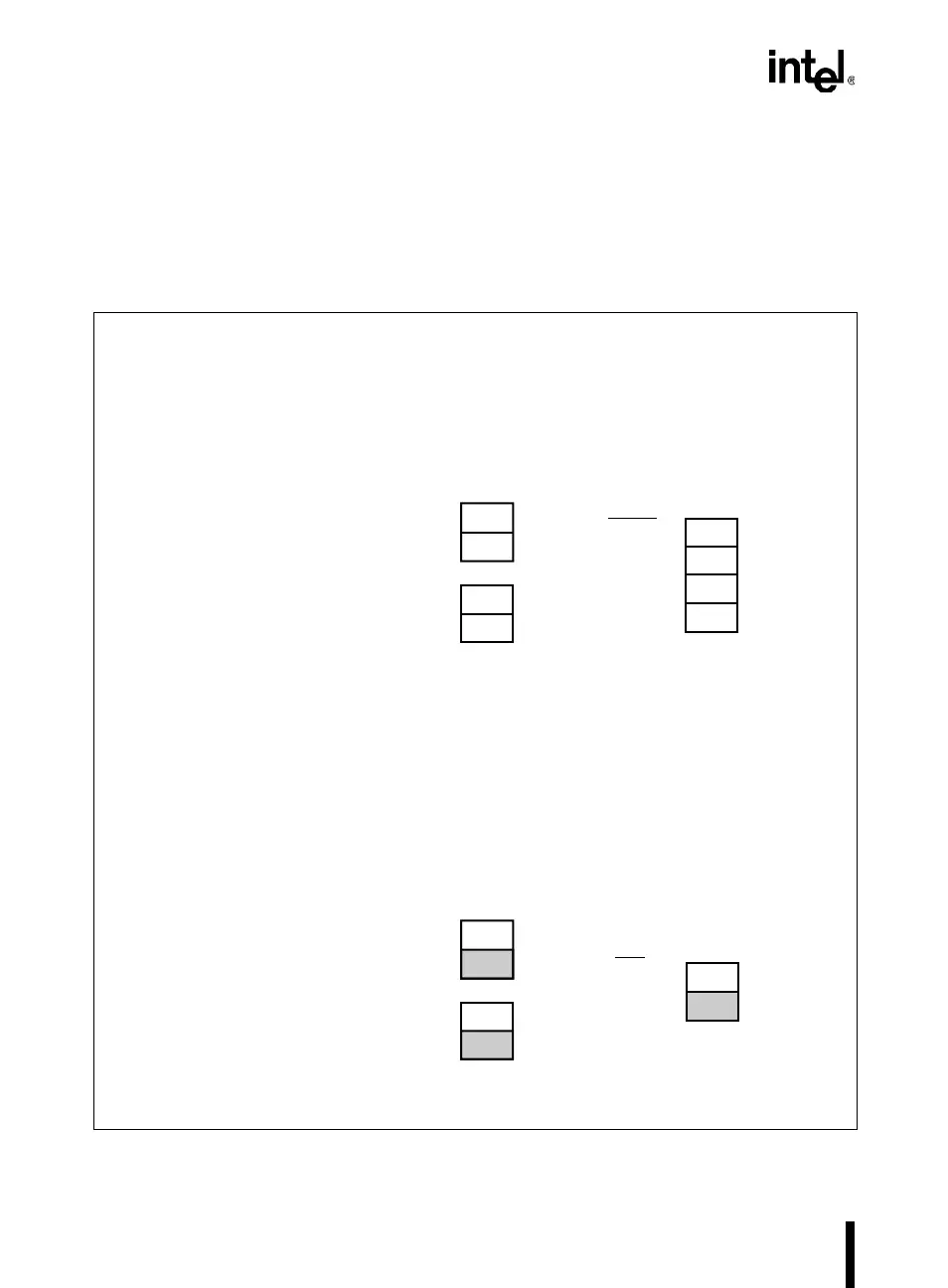
This selection provides a 128-Kbyte external address space. The advantage of this selection, in
comparison with the 256-Kbyte external memory space with RD1:0 = 00, is the availability of
pin P1.7/CEX4/A17/WCLK for general I/O, PCA I/O, and real-time wait clock output. I/O P3.7
is unavailable. All four 64-Kbyte regions are strobed by PSEN# and WR#. Sections 13.8.2 and
13.8.3 show examples of memory designs with this option.
Figure 4-5. Internal/External Address Mapping (RD1:0 = 00 and 01)
FF:
01:
PSEN#, WR#
PSEN#, WR#
A4218-02
FF:
FE:
01:
00:
RD1:0 = 00
18 external address bits:
P0, P2, A16, A17
PSEN#, WR#
PSEN#, WR#
01:, FF:
00:, FE:
01
FF:
FE:
00
256 Kbytes
128 Kbytes
Notes:
1. Maximum external
memory
2. Single read signal
Note:
Single read signal
Internal Memory with
Read/Write Signals
External
Memory
A16
1
0
RD1:0 = 01
A17:16
1 1
1 0
0 1
0 0
Internal Memory with
Read/Write Signals
External
Memory
17 external address bits:
P0, P2, A16
FE:
00: