C-17
REGISTERS
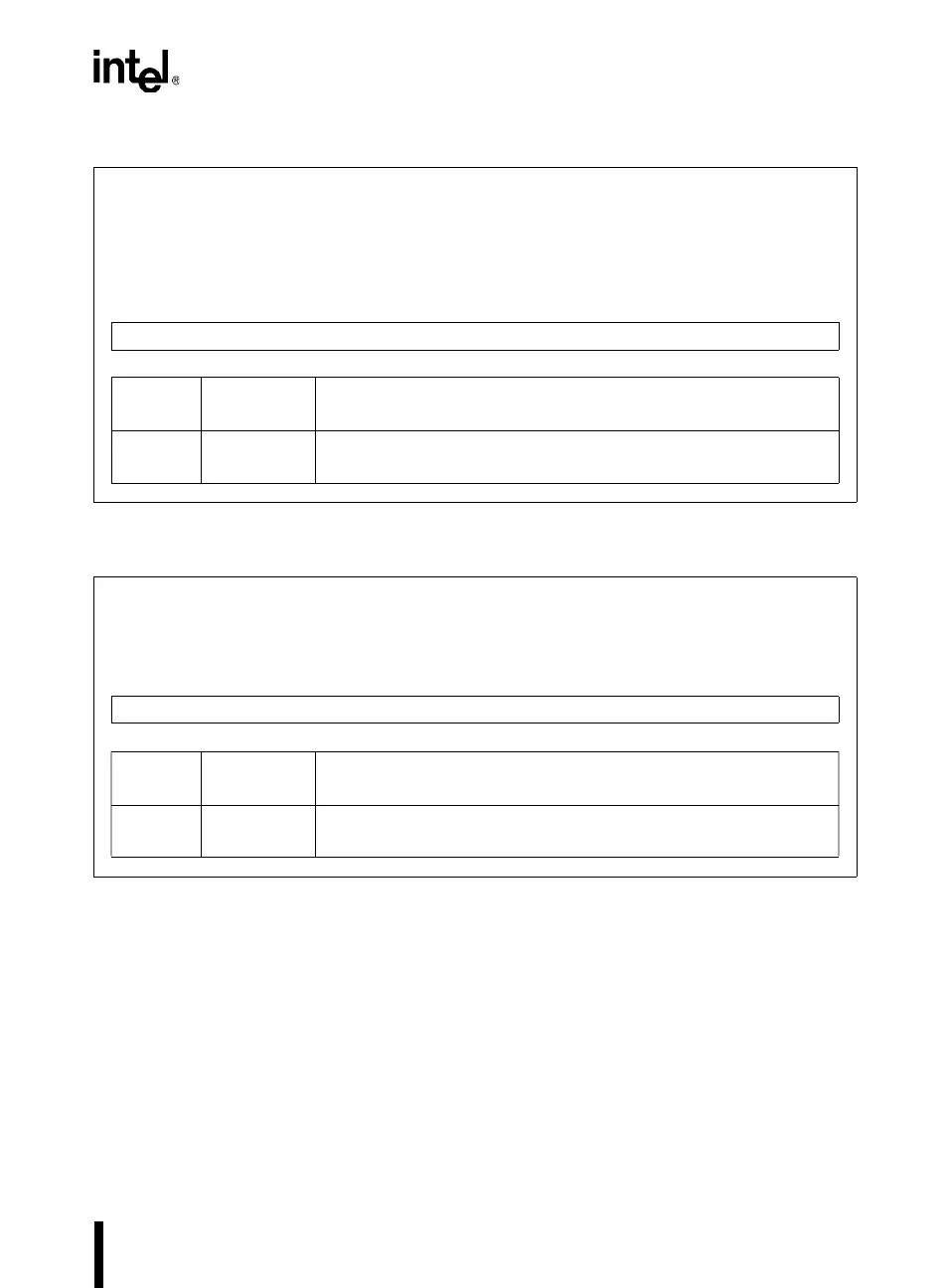
P0
Address: S:80H
Reset State: 1111 1111B
Port 0. P0 is the SFR that contains data to be driven out from the port 0 pins. Read-modify-write
instructions that read port 0 read this register. The other instructions that read port 0 read the port 0
pins. When port 0 is used for an external bus cycle, the CPU always writes FFH to P0, and the former
contents of P0 are lost.
7 0
P0 Contents
Bit
Number
Bit
Mnemonic
Function
7:0 P0.7:0 Port 0 Register:
Write data to be driven onto the port 0 pins to these bits.
P1
Address: S:90H
Reset State: 1111 1111B
Port 1. P1 is the SFR that contains data to be driven out from the port 1 pins. Read-write-modify
instructions that read port 1 read this register. Other instructions that read port 1 read the port 1 pins.
7 0
P1 Contents
Bit
Number
Bit
Mnemonic
Function
7:0 P1.7:0 Port 1 Register:
Write data to be driven onto the port 1 pins to these bits.
 Loading...


