Intel
®
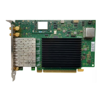
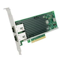
Ethernet Network Adapter E810-CQDA2T
User Guide
24 722960-002
# echo 0 0 > /sys/class/net/$ETH3/device/phy/synce
# dmesg
[27730.341153] ice 0000:03:00.3: Disabled recovered clock: pin C827_1-RCLKA
# echo 0 1 > /sys/class/net/$ETH4/device/phy/synce
# dmesg
[27730.341153] ice 0000:03:00.4: Disabled recovered clock: pin C827_1-RCLKB
Check recovered clock status. You can add the current status of the recovered clock to the dmesg:
#echo dump rclk_status > /sys/kernel/debug/ice/0000:03:00.0/command
# dmesg
[311274.298749] ice 0000:03:00.0: State for port 0, C827_0-RCLKA: Disabled
[311274.300060] ice 0000:03:00.0: State for port 0, C827_0-RCLKB: Disabled
Note: In secure boot case, check the pin_cfg file. For details, see Section 4.11.1.
Note: enp1s0f0, enp1s0f1, etc, refer to the physical function. In the case of the E810-CQDA2T
it has what is called inverted PF-to-Port mapping. This means that functions 0-3
correspond to quad 1 and functions 4-7 correspond to quad 0. The PHY lanes, that is the
physical Tx and Rx differential pairs, on the E810-CQDA2T are connected to the quad 0
and quad 1 cages. See the following table:
L4-L7 correspond to lanes 4 through 7, which correspond to quad 1. Therefore PF0-PF3
are driving quad 1. L0-L3 correspond to lanes 0 through 3, which correspond to quad 0.
Therefore PF4-PF7 are driving quad 0. For example if the desired recovered clock is from
L4, it corresponds to PF3.
Inverted Port Mapping
Physical Function PHY (Lane)
PF0 L7
PF1 L6
PF2 L5
PF3 L4
PF4 L3
PF5 L2
PF6 L1
PF7 L0