Datasheet 103
Electrical Specifications
NOTES:
1. V
TT
supplies the PECI interface. PECI behavior does not affect V
TT
min/max specifications.
2. The leakage specification applies to powered devices on the PECI bus.
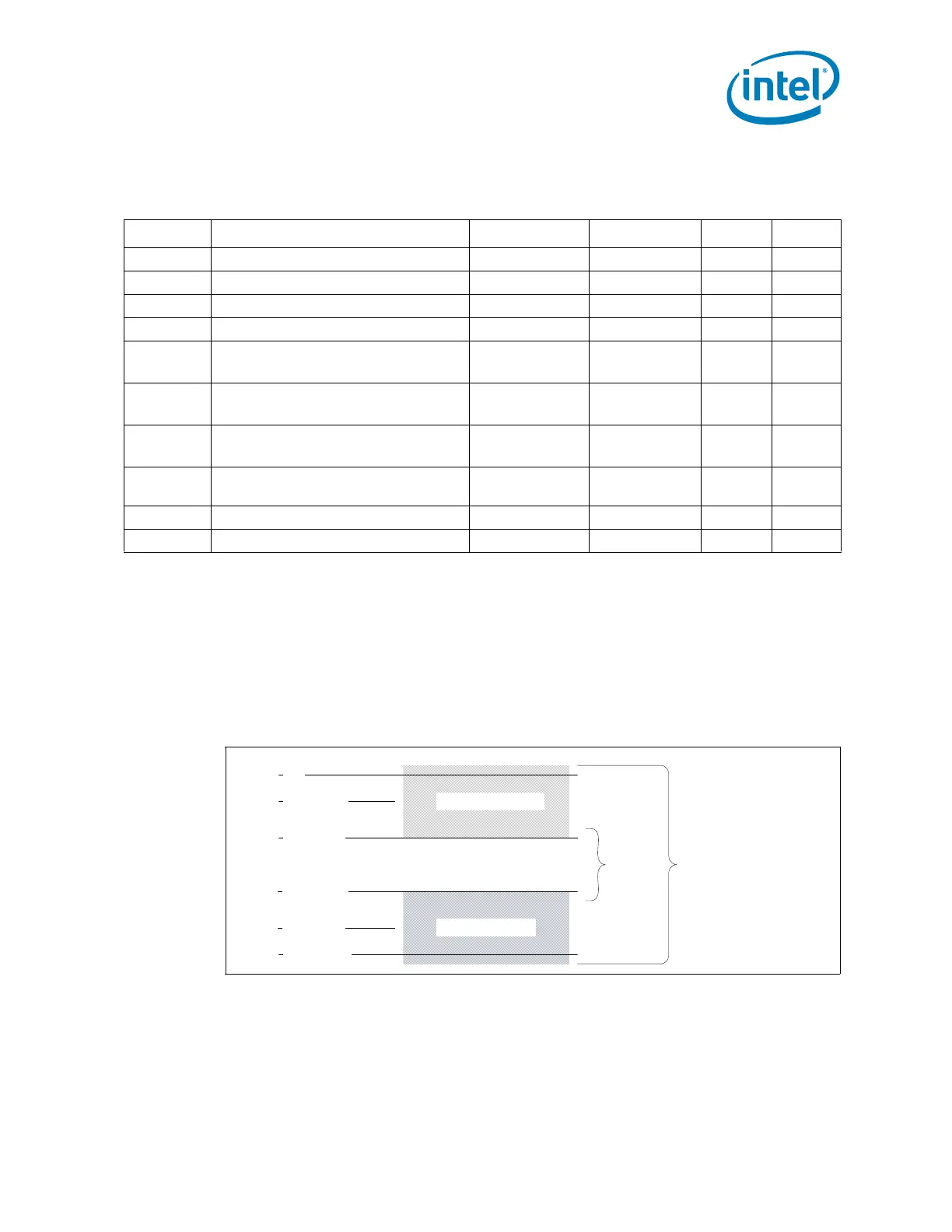
7.11.2 Input Device Hysteresis
The input buffers in both client and host models must use a Schmitt-triggered input
design for improved noise immunity. Use Figure 7-16 as a guide for input buffer design.
Table 7-48.PECI DC Electrical Limits
Symbol Definition and Conditions Min Max Units Notes
1
V
in
Input Voltage Range -0.150 V
TT
V
V
hysteresis
Hysteresis 0.1 * V
TT
N/A V
V
n
Negative-edge Threshold Voltage 0.275 * V
TT
0.500 * V
TT
V
V
p
Positive-edge Threshold Voltage 0.550 * V
TT
0.725 * V
TT
V
I
source
High-Level Output Source
(V
OH
= 0.75 * V
TT
)
-6.0 N/A mA
I
sink
Low-Level Output Sink
(V
OL
= 0.25 * V
TT
)
0.5 1.0 mA
I
leak+
High-Impedance State Leakage to V
TT
(V
leak
= V
OL
)
N/A 100 µA 2
I
leak-
High-Impedance Leakage to GND
(V
leak
= V
OH
)
N/A 100 µA 2
C
bus
Bus Capacitance Per Node N/A 10 pF
V
noise
Signal Noise Immunity above 300 MHz 0.1 * V
TT
N/A V
p-p
Figure 7-16.Input Device Hysteresis
Minimum V
P
Maximum V
P
Minimum V
N
Maximum V
N
PECI High Range
PECI Low Range
Valid Input
Signal Range
Minimum
Hysteresis
V
TTD
PECI Ground