Signal Description
70 Datasheet
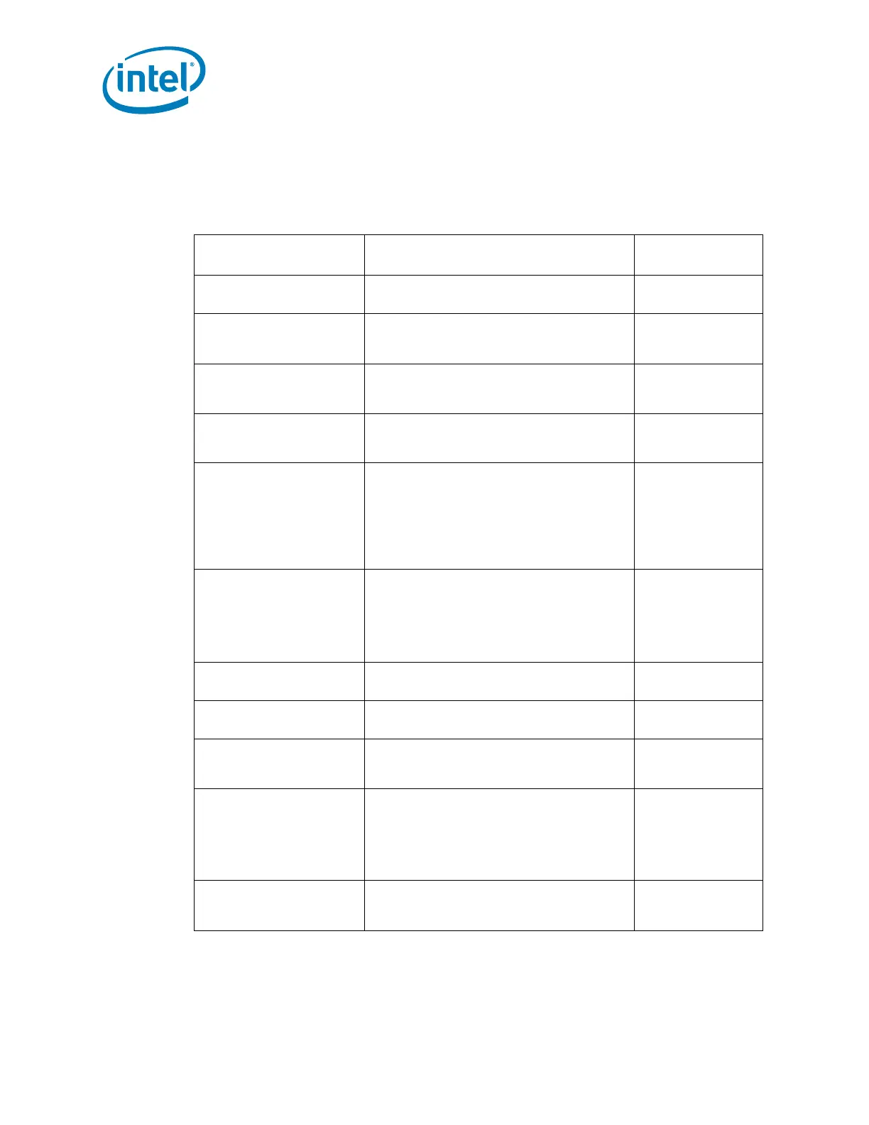
6.1 System Memory Interface
Table 6-22.Memory Channel A (Sheet 1 of 2)
Signal Name Description
Direction/Buffer
Type
SA_BS[2:0] Bank Select: These signals define which
banks are selected within each SDRAM rank.
O
DDR3
SA_WE# Write Enable Control Signal: Used with
SA_RAS# and SA_CAS# (along with
SA_CS#) to define the SDRAM Commands.
O
DDR3
SA_RAS# RAS Control Signal: Used with SA_CAS#
and SA_WE# (along with SA_CS#) to define
the SRAM Commands.
O
DDR3
SA_CAS# CAS Control Signal: Used with SA_RAS#
and SA_WE# (along with SA_CS#) to define
the SRAM Commands.
O
DDR3
SA_DM[7:0] Data Mask: These signals are used to mask
individual bytes of data in the case of a
partial write and to interrupt burst writes.
When activated during writes, the
corresponding data groups in the SDRAM are
masked. There is one SA_DM[7:0] for every
data byte lane.
O
DDR3
SA_DQS[7:0] Data Strobes: SA_DQS[7:0] and its
complement signal group make up a
differential strobe pair. The data is captured
at the crossing point of SA_DQS[7:0] and its
SA_DQS#[7:0] during read and write
transactions
I/O
DDR3
SA_DQS#[7:0] Data Strobe Complements: These are the
complementary strobe signals.
I/O
DDR3
SA_DQ[63:0] Data Bus: Channel A data signal interface to
the SDRAM data bus.
I/O
DDR3
SA_MA[15:0] Memory Address: These signals are used to
provide the multiplexed row and column
address to the SDRAM.
O
DDR3
SA_CK[1:0] SDRAM Differential Clock: Channel A
SDRAM Differential clock signal pair. The
crossing of the positive edge of SA_CK and
the negative edge of its complement
SA_CK# are used to sample the command
and control signals on the SDRAM.
O
DDR3
SA_CK#[1:0] SDRAM Inverted Differential Clock:
Channel A SDRAM Differential clock signal-
pair complement.
O
DDR3