Intel® Server Board S1200SP Family Technical Product Specification
xi
List of Figures
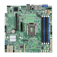
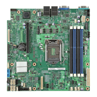
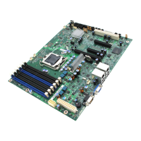
Figure 1. Intel
®
Server Board S1200SP Layout (S1200SPL) ..................................................................................................... 4
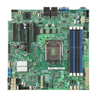
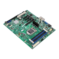
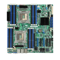
Figure 2. Intel
®
Server Board S1200SPL Layout ......................................................................................................................... 5
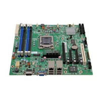
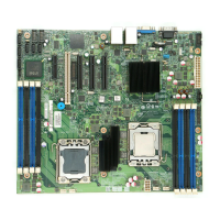
Figure 3. Intel
®
Server Board S1200SPS Layout ........................................................................................................................ 6
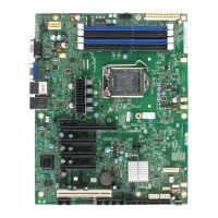
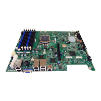
Figure 4. Intel
®
Server Board S1200SPO Layout ........................................................................................................................ 7
Figure 5. Intel
®
Server Board S1200SP – Mounting Hole Locations ........................................................................................ 8
Figure 6. Intel® Server Board S1200SP – Mounting Hole Locations (continued) .................................................................. 9
Figure 7. Intel
®
Server Board S1200SP – Major Connector Pin-1 Locations ........................................................................ 10
Figure 8. Intel® Server Board S1200SP – Major Connector Pin-1 Locations (continued) .................................................. 11
Figure 9. Intel® Server Board S1200SP – Primary Side Keepout Zone ................................................................................. 12
Figure 10. Intel® Server Board S1200SP – Second Side Keepout Zone ............................................................................... 13
Figure 11. Intel
®
Server Board S1200SPL Rear I/O Layout ..................................................................................................... 14
Figure 12. Intel
®
Server Board S1200SPS Rear I/O Layout ..................................................................................................... 14
Figure 13. Intel
®
Server Board S1200SPO Rear I/O Layout .................................................................................................... 14
Figure 13. Intel
®
Server Board S1200SP Functional Block Diagram ..................................................................................... 15
Figure 14. Intel
®
Server Board S1200SP DIMM Slot Layout ................................................................................................... 20
Figure 15. Intel® Server Board S1200SP Series USB Mapping Diagram............................................................................... 26
Figure 16. Integrated BMC Functional Block Diagram ............................................................................................................ 30
Figure 17. Setup Utility – TPM Configuration Screen ............................................................................................................. 36
Figure 18. Fan Speed Control Process ...................................................................................................................................... 49
Figure 19. Intel
®
RMM4 Lite Activation Key Installation ......................................................................................................... 66
Figure 20. Installing M.2 Device ................................................................................................................................................. 78
Figure 21. Installing Intel
®
Integrated RAID Module ............................................................................................................... 82
Figure 22. Fan Headers on the Server Borad ........................................................................................................................... 84
Figure 23. Jumper Blocks (J4B1, J1F1, J1F4 J7B1, J4C1) ..................................................................................................... 85
Figure 24. On-Board LED Placement ......................................................................................................................................... 90
Figure 25. Power Distribution Block Diagram .......................................................................................................................... 96
Figure 26. Differential Noise Test Setup ................................................................................................................................... 99
Figure 27. Turn On/Off Timing (Power Supply Signals) ....................................................................................................... 101
Figure 28. POST Code Diagnostic LEDs .................................................................................................................................. 120
Figure 29. Processor Heatsink Installation ............................................................................................................................ 129