PRINCIPLES OF OPERATION
5.3.2 Multiplexer
Figure 5-5 shows the general switching phases for the
various signals. During each phase, an integration is per-
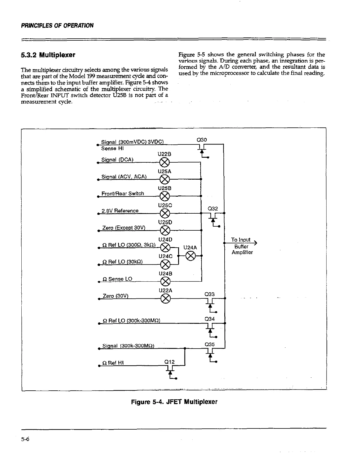
The multiplexer circuitry selects among the v&xzs signals
formed by the A/D converter, and the resultant data is
that are part of the Model 159 measwement cycle and con-
used by the microprocessor to calculate the final reading.
nects them to the input buffer amplifier. Figure 54 shows
a simplified schematic of the multiplexer circuitry. The
Front/Rear INPUT switch detector U25B is not part of a
measurement cycle.
) R Ref LO (300k-300MR)
Siqnal (300k-300MQ)
Q35
QRl?f HI
(112
Figure 5-4. JFET Multiplexer
5-6