Troubleshooting
2-102
Test 408.3 – ÷200 correction factor; setup for test
408.5 and A/D measurement
for test 408.6
Circuit Exercise
The DAC (U531) is programmed with Ò0sÓ (full compensation) and OUT A is routed
to C554. The signal at BUFF is routed through R233 and applied to NET1 (R557). The
voltage at pin 4 of NET1 is routed through U526 (DCF pulled low) and Q516, and ap-
plied to the input buffer (Q512 and U520). The buffered signal is tied to AMP IN.
The signal at AMP IN is then routed to Q510 via U522 (SELFTEST1 pull low) and the
x5 inverting ampliÞer (U523, R542 and R533).
The voltage on C529 is buffered by Q505 and tied to SELFTEST OUT. The signal at
SELFTEST OUT is then switched through multiplexer U511. The output (OUT) of the
multiplexer is routed through buffer U342 to ACV/A. The signal at ACV/A is routed
through U320 (/AC pulled low) and applied to the A/D buffer (U322), which is con-
Þgured for x1 gain.
Measure the output at A/D IN.
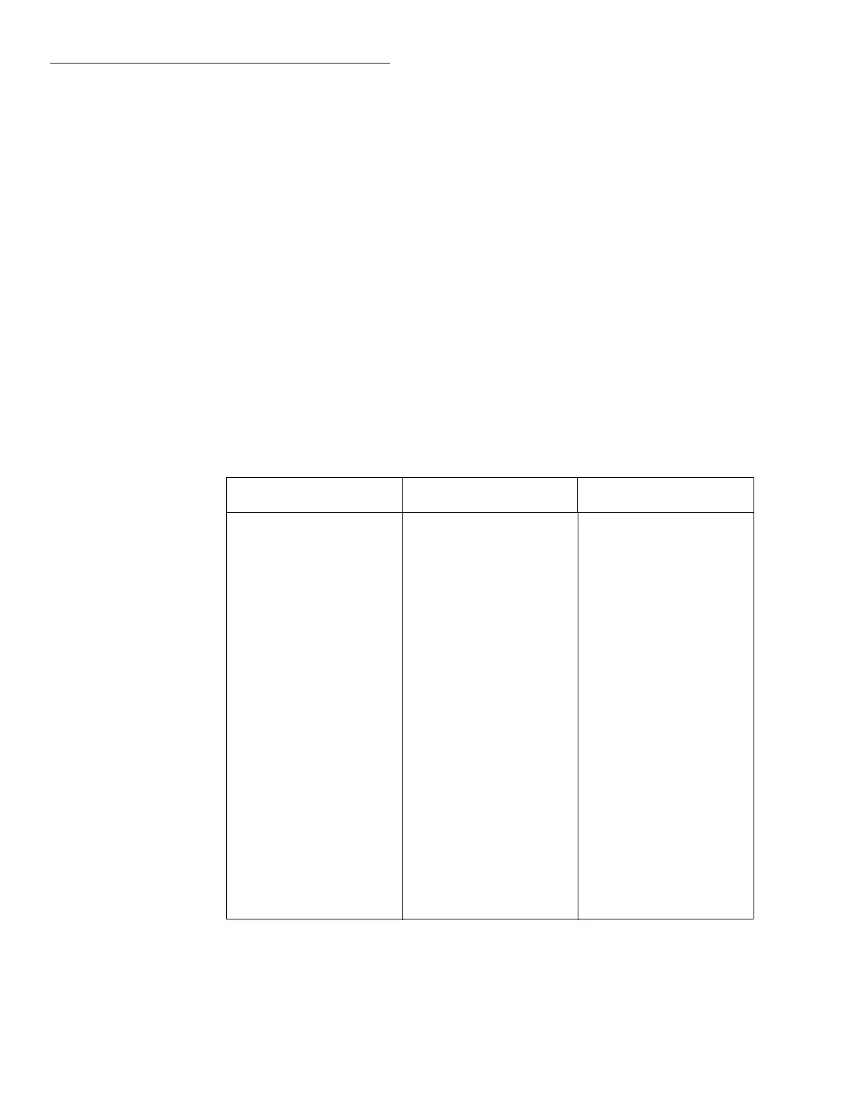
DC_STB
Registers
R1_STB
Registers
R2_STB
Registers
U801 Q1: 0
Q2: 1
Q3: 1
Q4: 1
Q5: 1
Q6: 0
Q7: 0
Q8: 0
U307 Q1: 1
Q2: 1
Q3: 0
Q4: 1
Q5: 1
Q6: 1
Q7: 1
Q8: 1
U505 Q1: 0
Q2: 1
Q3: 1
Q4: 1
Q5: 0
Q6: 1
Q7: 1
Q8: 0
U800 Q1: 1
Q2: 1
Q3: 0
Q4: 0
Q5: 0
Q6: 0
Q7: 1
Q8: 1
U305 Q1: 1
Q2: 0
Q3: 1
Q4: 0
Q5: 0
Q6: 0
Q7: 1
Q8: 1
U500 Q1: 1
Q2: 1
Q3: 0
Q4: 1
Q5: 1
Q6: 1
Q7: 0
Q8: 0
U300 Q1: 1
Q2: 1
Q3: 1
Q4: 1
Q5: 1
Q6: 1
Q7: 1
Q8: 1
U302 Q1: 1
Q2: 1
Q3: 1
Q4: 1
Q5: 1
Q6: 1
Q7: 1
Q8: 0
U530 Q1: 0
Q2: 0
Q3: 0
Q4: 0
Q5: 0
Q6: 0
Q7: 0
Q8: 0
U303 Q1: 0
Q2: 1
Q3: 1
Q4: 1
Q5: 0
Q6: 1
Q7: X
Q8: X
U501 Q1: 1
Q2: 0
Q3: 1
Q4: 1
Q5: 1
Q6: 1
Q7: X
Q8: X
Note: Tables 2-10 through 2-12 provide functional descriptions of the register bits.
Type
Description
Bit pattern

 Loading...


