EasyManuals Logo

Lattice Semiconductor CrossLink-NX User Manual

Lattice Semiconductor CrossLink-NX
58 pages
To Next Page IconTo Next Page
To Previous Page IconTo Previous Page
Page #5 background image
CrossLink-NX Evaluation Board
User Guide
© 2019-2020 Lattice Semiconductor Corp. All Lattice trademarks, registered trademarks, patents, and disclaimers are as listed at www.latticesemi.com/legal.
All other brand or product names are trademarks or registered trademarks of their respective holders. The specifications and information herein are subject to change without notice.
FPGA-EB-02028-1.3 5
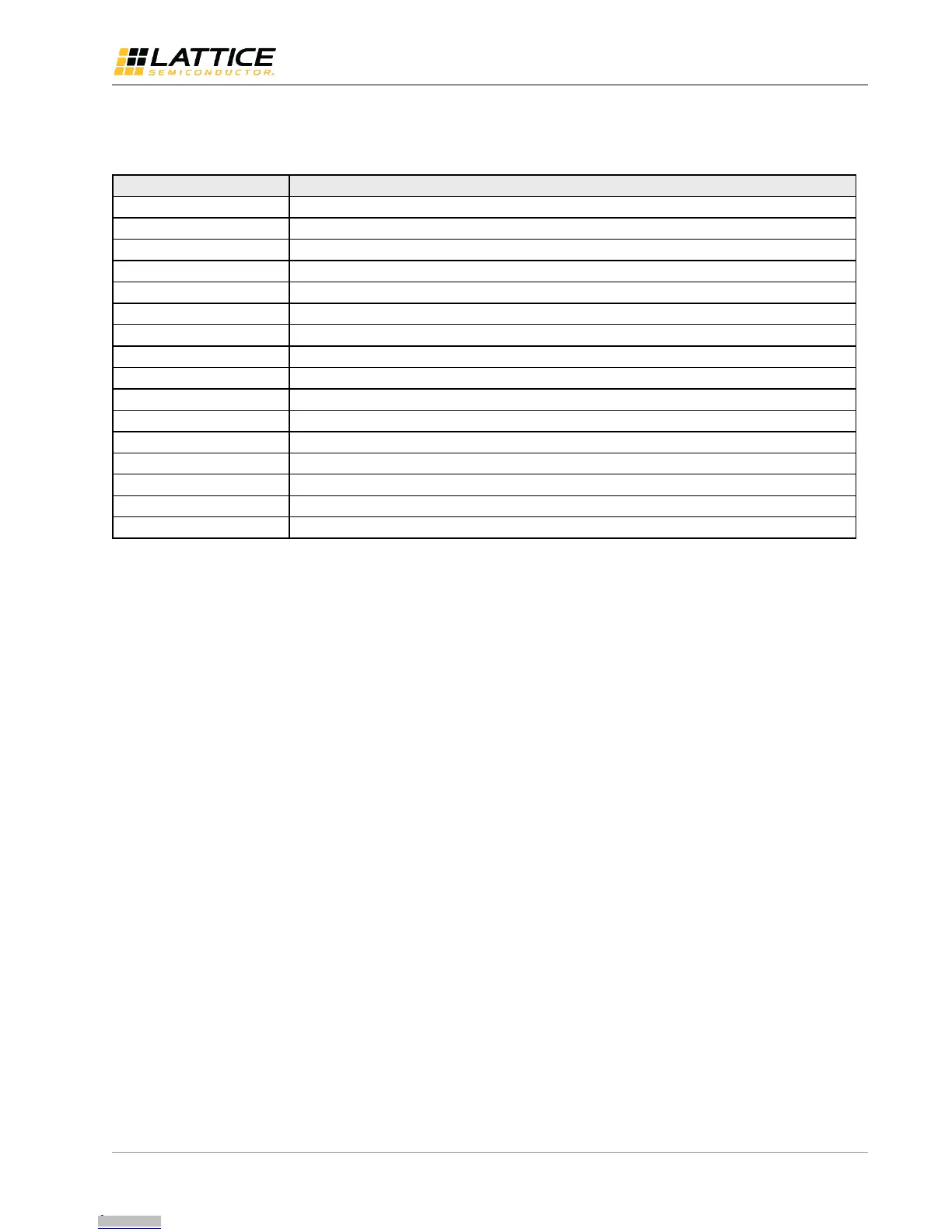
Acronyms in This Document
A list of acronyms used in this document.
Acronym
Definition
caBGA
Chip Array Ball Grid Array
CMOS
Complementary Metal-Oxide Semiconductor
DIP
Dual Inline Package
DNI
Do Not Install
ESD
Electro Static Discharge
FMC LPC
FPGA Mezzanine Low Pin Count Connector
FPGA
Field Programmable Logic Array
FTDI
Future Technology Devices International
GPIO
General Purpose Input/Output
I
2
C
Inter-Integrated Circuit
JTAG
Joint Test Action Group
LVDS
Low-Voltage Differential Signaling
PMOD
Peripheral Module
SPI
Serial Peripheral Interface
UART
Universal Asynchronous Receiver Transmitter
USB
Universal Serial Bus
Downloaded from Arrow.com.Downloaded from Arrow.com.Downloaded from Arrow.com.Downloaded from Arrow.com.Downloaded from Arrow.com.

Table of Contents

Other manuals for Lattice Semiconductor CrossLink-NX

Questions and Answers:

Question and Answer IconNeed help?

Do you have a question about the Lattice Semiconductor CrossLink-NX and is the answer not in the manual?

Lattice Semiconductor CrossLink-NX Specifications

General IconGeneral
BrandLattice Semiconductor
ModelCrossLink-NX
CategoryMotherboard
LanguageEnglish

Related product manuals