CrossLink-NX Evaluation Board
User Guide
© 2019-2020 Lattice Semiconductor Corp. All Lattice trademarks, registered trademarks, patents, and disclaimers are as listed at www.latticesemi.com/legal.
All other brand or product names are trademarks or registered trademarks of their respective holders. The specifications and information herein are subject to change without notice.
FPGA-EB-02028-1.3 9
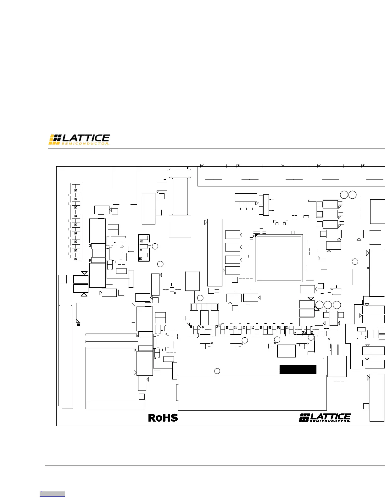
Figure 1.3. Silkscreen of CrossLink-NX Evaluation Board
D27
D25
R119
R126
D23
R125
R117
D26
D24
R118
D21
D22
R115
D19
D20
R114
JP5
JP3
JP4
L15
SW1
D32
D31
C141
L14
R121
D30
R153
R152
J40
J39
C154
J41
C145
D29
C144
C151
C152
TP_V5P0
L17
D36
C155
D35
R162
J42
TP_V3P3
C142
C143
R160
R155
R159
C146
C147
C149
R151
U15
R154
R156
R157
TP_V1P8
J43
D18
J33
D17
D1
R76
X2
F1
D34
C170
R163
C159
U16
D33
C158
C165
L16
C166
TP_VCC_CORE_V1P0
R145
C135
R140
TP12
TP10
TP_V2P8
TP_V1P2
R24
CN1
C157
C156
C163
R165
R170
R168
C161
R161
R150
R169
R164
FB8
J36
C137
U14
R141
C167
D16
R187
C160
R166
C164
J35
J34
TP_VCCIO3
TP_VCCIO4
TP_VCCIO5
R77
C76
D15
R186
TP13
TP_V1P0_LDO
R80
D13
D14
SW4
SW5
R185
R149
FB7
J32
TP_VCCIO7
J6
D12
R184
J31
FB6
TP_VCCIO6
C39
R36
J3
J5
J4
C32
L4
L8
L6
J13
J14
R72
C63
C61
D11
D10
R67
R69
TP7
R182
R183
C134
R40
R35
R39
C68
U3
C133
C122
R27
R28
R30
C26
C30
R70
SW2
D8
D9
R180
R181
J38
R31
R66
C48
L10
R29
C56
L11
J10
D4
R174
R175
TP6
D7
R178
R179
R49
R52
R51
R48
R47
R56
C57
C49
R62
R50
D3
C102
R68
C105
D6
SW3
D5
R176
R177
JP8
JP6
JP7
J23
R41
R46
R65
R54
C55
C54
R64R61
R59
R63
R60
C62
U10
R71
TP8
C88
R102
C64
R37
R74
R73
R75
TP_VCCIO0
C53
C50
TP_V1P0_VCCSD
R57
R58
R55
TP_V1P8_VCCPLLSD
TP_V1P8_VCCAUXSD
J16
C100
L13
U9
J30
C139
R143
TP_V1P8_LDO
RN1
R38
R111
R109
C99
C97
R110
R112
J29
TP5
R148
U13
C136
J37
J28
J7
J8
FB2
FB1
J9
FB3
TP2
J12
TP_VADJ
C104
C103
C101
R108
C98
C82
U7
J25
L12
TP_VCCIO1
TP_VCCIO2
TP4
TP3
U6
TP9
R21
J44
R18
R20
R17
R15
TP1
J21
J22
C89
J24
J20
R19
J27
R99
C90
R98
U2
U1
J15
J26
J1
C16
R9
C17
X1
JP1
U8
D2
J2
J19
J18
J17
JP2
J11
H40
C40
49
48
33
32
BOARD EDGE
64
16
17
1
30
ON
16
15
H1
C1
JTAG
1
RXDP
POT
PMOD2
1
PMOD1
1
PMOD0
1
USB
MINI
1
ADC
1
FMC CONFIG
1
RXDN
FLASH/FPGA
1
TXDP
PB1
TXDN
CrossLink-NX Evaluation Board
LIFCL-40-EVN REV B
Copyright C 2019
PROG
MIPI CSI-2
FPGA MEZZANINE CARD
D-PHY 1
1
CLKN
GSRN
11
CLKP
MADE IN USA
DEMO LEDS
CROSSLINK NX
PBO
SERDES
1
39
1
40
RASPBERRY PI AND USER I/O
1.8V
3.3V
2
POWER LEDS
PROTOTYPE AREA
DEMO SW
1.0V
1.0VL
1.8VL
1.2V
2.8V
1.8V
3.3V
12V
5V
3
GND
LEDS
STATUS
1
RPI/USER
1.8V/3.3V
INITN
DONE
ACT
POWER
2
Downloaded from Arrow.com.Downloaded from Arrow.com.Downloaded from Arrow.com.Downloaded from Arrow.com.Downloaded from Arrow.com.Downloaded from Arrow.com.Downloaded from Arrow.com.Downloaded from Arrow.com.Downloaded from Arrow.com.