Multiformat Video Encoder
Six, 11-Bit, 297 MHz DACs
ADV7342/ADV7343
Rev. 0
In form atio n fu rnis hed by A nalo g Dev ices i s bel ieve d to b e acc urat e a nd r elia ble. H oweve r, no
res pon sibi lit y i s a ssu med by Ana log De vice s f or its us e, nor for a ny i nfr inge men ts of pate nts or ot her
rights of third par ties that may result from its use. Specifications subject to change with out n otice. N o
li cens e is gran ted by im pli cati on o r ot her wis e un der a ny p aten t or pate nt r ight s of Anal og D evi ces.
Trad ema rks and re gist ere d tr ade mar ks a re the pro per ty of the ir resp ec tive ow ners .
One Technology Way, P.O. Box 9106, Norwood, MA 02062-9106, U.S.A.
Tel: 781.329.4700
www.analog.com
Fax: 781.461.3113 ©2006 Analog Devices, Inc. All rights reserved.
FEATURES
74.25 MHz 20-/30-bit high definition input support
Compliant with SMPTE 274M (1080i), 296M (720p),
and 240M (1035i)
6, 11-bit, 297 MHz video DACs
16× (216 MHz) DAC oversampling for SD
8× (216 MHz) DAC oversampling for ED
4× (297 MHz) DAC oversampling for HD
37 mA maximum DAC output current
NTSC M, PAL B/D/G/H/I/M/N, PAL 60 support
NTSC and PAL square pixel operation (24.54 MHz/29.5 MHz)
Multiformat video input support
4:2:2 YCrCb (SD, ED, and HD)
4:4:4 YCrCb (ED and HD)
4:4:4 RGB (SD, ED, and HD)
Multiformat video output support
Composite (CVBS) and S-Video (Y/C)
Component YPrPb (SD, ED, and HD)
Component RGB (SD, ED, and HD)
Macrovision® Rev 7.1.L1 (SD) and Rev 1.2 (ED) compliant
Simultaneous SD and ED/HD operation
EIA/CEA-861B compliance support
Programmable features
Luma and chroma filter responses
Vertical blanking interval (VBI)
Subcarrier frequency (F
SC
) and phase
Luma delay
Copy generation management system (CGMS)
Closed captioning and wide screen signaling (WSS)
Integrated subcarrier locking to external video source
Complete on-chip video timing generator
On-chip test pattern generation
On-board voltage reference (optional external input)
Serial MPU interface with dual I
2
C® and SPI® compatibility
3.3 V analog operation
1.8 V digital operation
3.3 V I/O operation
Temperature range: −40°C to +85°C
APPLICATIONS
DVD recorders and players
High definition Blu-ray DVD players
HD-DVD players
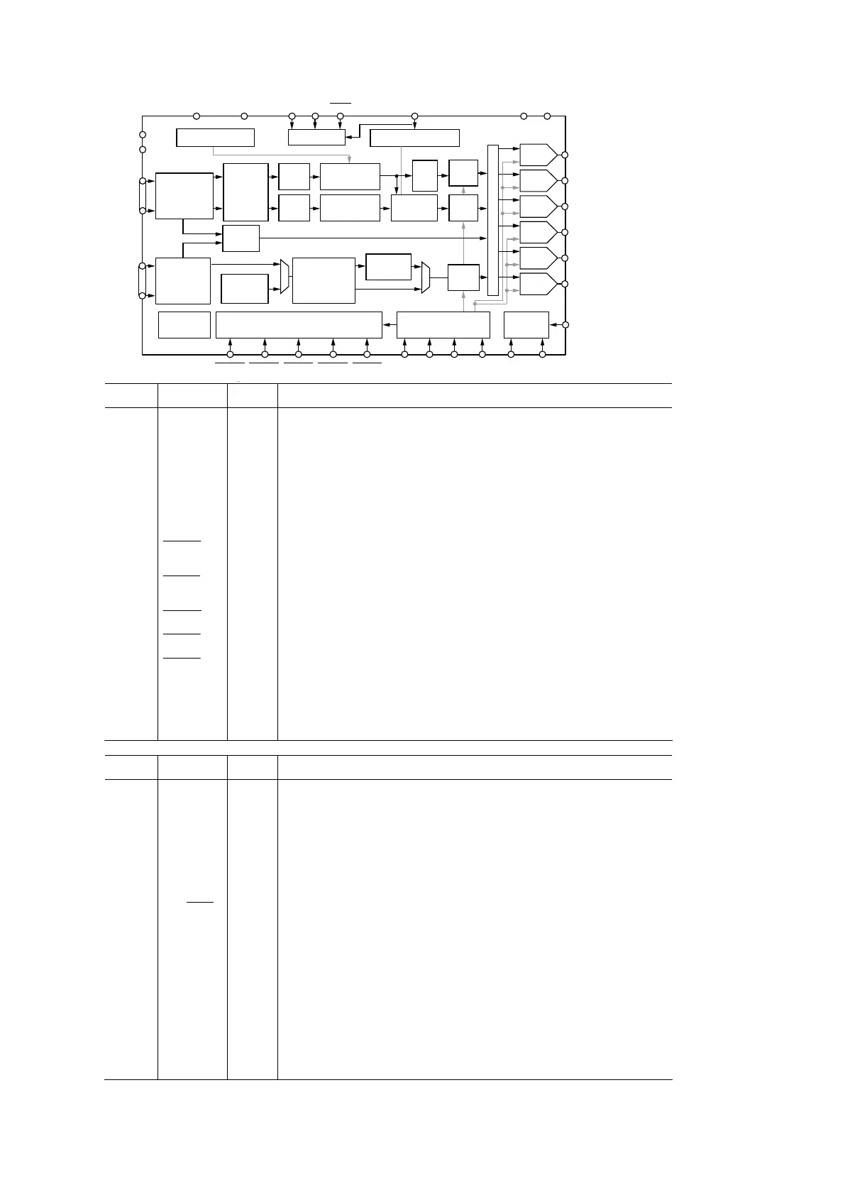
FUNCTIONAL BLOCK DIAGRAM
Figure 1.
Protected by U.S. Patent Numbers 5,343,196 and 5,442,355 and other intellectual property rights.
Protected by U.S. Patent Numbers 4,631,603, 4,577,216, 4,819,098 and other intellectual property rights.
ADV7342/ADV7343
Rev. 0 | Page 18 of 88
PIN CONFIGURATION AND FUNCTION DESCRIPTIONS
Figure 21. Pin Configuration
Table 13. Pin Function Descriptions
Pin No. Mnemonic
Input/
Output
Description
13, 12,
9 to 4
Y7 to Y0 I 8-Bit Pixel Port. Y0 is the LSB. Refer to Table 31 for input modes.
29 to 25,
18 to 16
C7 to C0 I 8-Bit Pixel Port. C0 is the LSB. Refer to Table 31 for input modes.
62 to 58,
55 to 53
S7 to S0 I 8-Bit Pixel Port. S0 is the LSB. Refer to Table 31 for input modes.
52, 51, 15,
14, 3, 2
TEST5 to
TEST0
I Unused. These pins should be connected to DGND.
30 CLKIN_A I Pixel Clock Input for HD Only (74.25 MHz), ED
1
Only (27 MHz or 54 MHz) or SD Only (27 MHz).
63 CLKIN_B I
Pixel Clock Input for Dual Modes Only. Requires a 27 MHz reference clock for ED operation or a
74.25 MHz reference clock for HD operation.
50
S_HSYNC
I/O
SD Horizontal Synchronization Signal. This pin can also be configured to output an SD, ED, or HD
horizontal synchronization signal. See the External Horizontal and Vertical Synchronization
Control section.
49
S_VSYNC
I/O
SD Vertical Synchronization Signal. This pin can also be configured to output an SD, ED, or HD
vertical synchronization signal. See the External Horizontal and Vertical Synchronization Control
section.
22
P_HSYNC
I
ED/HD Horizontal Synchronization Signal. See the External Horizontal and Vertical
Synchronization Control section.
23
P_VSYNC
I
ED/HD Vertical Synchronization Signal. See the External Horizontal and Vertical Synchronization
Control section.
24
P_BLANK
I ED/HD Blanking Signal. See the External Horizontal and Vertical Synchronization Control section.
48 SFL/MISO I/O
Multifunctional Pin: Subcarrier Frequency Lock (SFL) Input/SPI Data Output. The SFL input is
used to drive the color subcarrier DDS system, timing reset, or subcarrier reset.
47 R
SET1
I
This pin is used to control the amplitudes of the DAC 1, DAC 2, and DAC 3 outputs. For full-drive
operation (for example, into a 37.5 Ω load), a 510 Ω resistor must be connected from R
SET1
to
AGND. For low drive operation (for example, into a 300 Ω load), a 4.12 kΩ resistor must be
connected from R
SET1
to AGND.
ADV7342/ADV7343
Rev. 0 | Page 19 of 88
Pin No. Mnemonic
Input/
Output Description
36 R
SET2
I
This pin is used to control the amplitudes of the DAC 4, DAC 5, and DAC 6 outputs. A 4.12 kΩ
resistor must be connected from R
SET2
to AGND.
45, 35
COMP1,
COMP2
O Compensation Pins. Connect a 2.2 nF capacitor from both COMP pins to V
AA
.
44, 43, 42
DAC 1, DAC 2,
DAC 3
O DAC Outputs. Full and low drive capable DACs.
39, 38, 37
DAC 4, DAC 5,
DAC 6
O DAC Outputs. Low drive only capable DACs.
21 SCL/MOSI I Multifunctional Pin: I
2
C Clock Input/SPI Data Input.
20 SDA/SCLK I/O Multifunctional Pin: I
2
C Data Input/Output. Also, SPI clock input.
19
ALSB/SPI_SS
I Multifunctional Pin: This signal sets up the LSB
2
of the MPU I
2
C address. Also, SPI slave select.
46 V
REF
Optional External Voltage Reference Input for DACs or Voltage Reference Output.
41 V
AA
P Analog Power Supply (3.3 V).
10, 56 V
DD
P
Digital Power Supply (1.8 V). For dual-supply configurations, V
DD
can be connected to other 1.8 V
supplies through a ferrite bead or suitable filtering.
1 V
DD_IO
P Input/Output Digital Power Supply (3.3 V).
34 PV
DD
P
PLL Power Supply (1.8 V). For dual-supply configurations, PV
DD
can be connected to other 1.8 V
supplies through a ferrite bead or suitable filtering.
33 EXT_LF1 I External Loop Filter for On-Chip PLL 1.
31 EXT_LF2 I External Loop Filter for On-Chip PLL 2.
32 PGND G PLL Ground Pin.
40 AGND G Analog Ground Pin.
11, 57 DGND G Digital Ground Pin.
64 GND_IO G Input/Output Supply Ground Pin.
1
ED = enhanced definition = 525p and 625p.
2
LSB = least significant bit. In the ADV7342, setting the LSB to 0 sets the I
2
C address to 0xD4. Setting it to 1 sets the I
2
C address to 0xD6. In the ADV7343, setting the
LSB to 0 sets the I
2
C address to 0x54. Setting it to 1 sets the I
2
C address to 0x56.
IC32 : ADV7342