DESCRIPTION
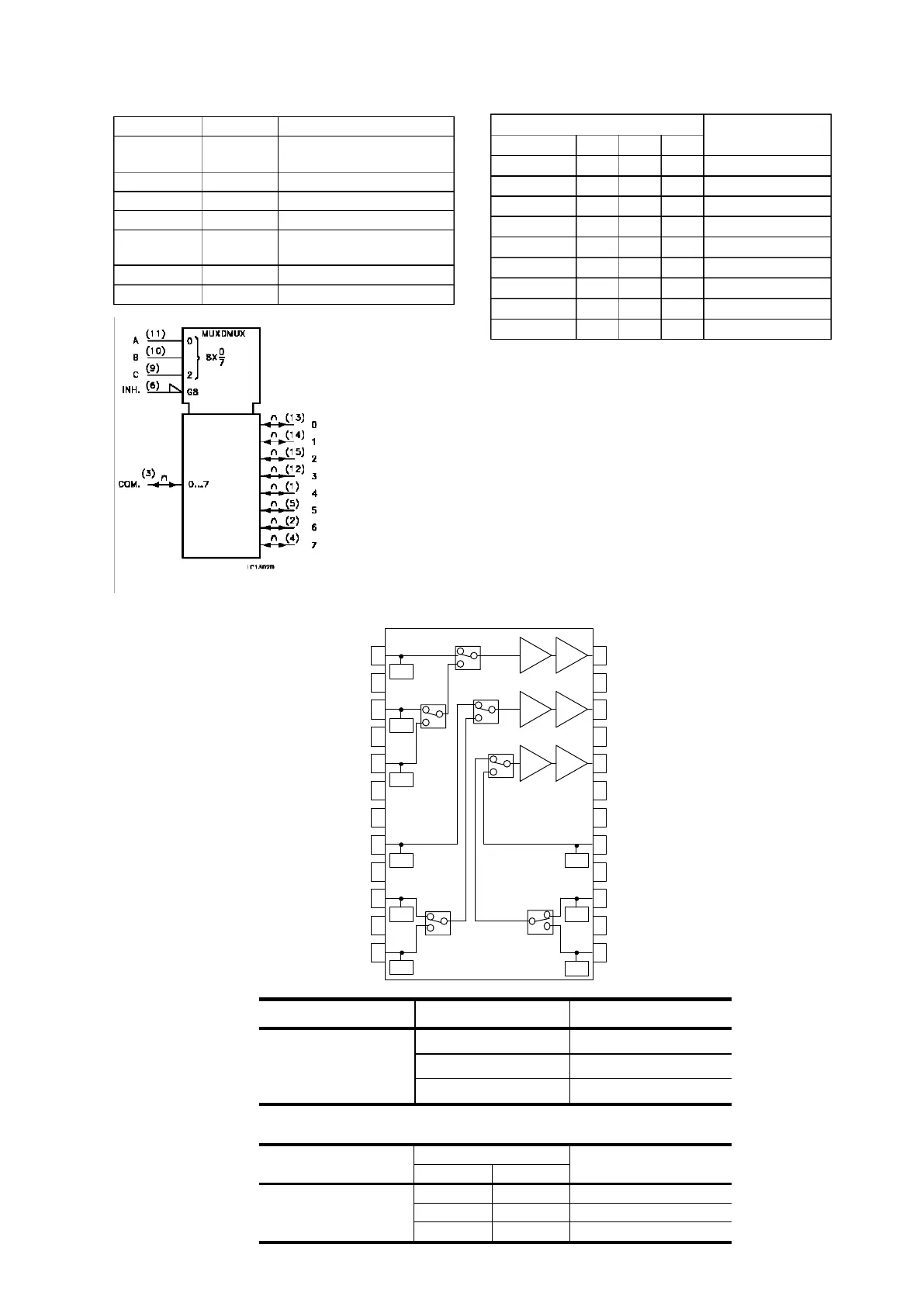
The HC4051 is a single 8 channel multiplexer
demultiplexer having three binarycontrol inputs A,
B and C to select 1 of 8 to be turned on, and
connected to theoutput.
The HC4052has a pair of fourchannel multiplexer
demultiplexer havingtwocontrolinputsAand Bthat
selectone of four channels of the two sections.
The HC4053 is a triple two channel multiplexer
demultiplexer havingthree separate digitalcontrol
inputs A, B and C to select independently oneof a
pairof channles.
CHIP CARRIER
HC4053HC4052HC4051
TRUTH TABLE (HC4051)
INPUT STATES
”ON” CHANNEL
INHIBIT C B A
L LLL 0
L LLH 1
L LHL 2
L LHH 3
L HLL 4
L HLH 5
L HHL 6
L HHH 7
H X X X NONE
X: DON’T CARE
TRUTH TABLE (HC4052)
INPUT STATES
”ON” CHANNELS
INHIBIT B A
L L L 0X, 0Y
L L H 1X, 1Y
L H L 2X, 2Y
L H H 3X, 3Y
H X X NONE
X: DON’T CARE
TRUTH TABLE (HC4053)
INPUT STATES
”ON” CHANNELS
INHIBIT A or B or C
L L ax or bx or cx
L H ay or by or cy
H X NONE
X: DON’T CARE
M54/M74HC4051/4052/4053
2/15
IEC LOGIC SYMBOLS
HC4053HC4052HC4051
PIN DESCRIPTION (HC4051)
PIN No SYMBOL NAME AND FUNCTION
3 COM
OUT/IN
Common Output/input
6 INH INHIBIT Input
7V
EE
Negative Supply Voltage
11, 10, 9 A, B, C Select Inputs
13, 14, 15,
12, 1, 5, 2, 4
0 TO 7 Independent Input/Outputs
8 GND Ground (0V)
16 V
CC
Positive Supply Voltage
PIN DESCRIPTION (HC4053)
PIN No SYMBOL NAME AND FUNCTION
2, 1 bx, by Independent Input/Outputs
5, 3 cx, cy Independent Input/Outputs
6 INH INHIBIT Input
7V
EE
Negative Supply Voltage
11, 10, 9 A, B, C Select Inputs
12, 13 ax, ay Independent Input/Outputs
14, 15, 4 ax TO cy Common Output/input
8 GND Ground (0V)
16 V
CC
Positive Supply Voltage
PIN DESCRIPTION (HC4052)
PIN No SYMBOL NAME AND FUNCTION
1, 5, 2, 4 0Y TO 3Y Independent Input/Outputs
6 INH INHIBIT Input
7V
EE
Negative Supply Voltage
10, 9 A, B Select Inputs
12, 14, 15,
11
0X TO 3X Independent Input/Outputs
3 COM Y
OUT/IN
Common X Output/input
13 COM X
OUT/IN
Common Y Output/input
8 GND Ground (0V)
16 V
CC
Positive Supply Voltage
M54/M74HC4051/4052/4053
3/15
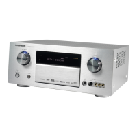
NJM2586A
WIDE BAND 3-INPUT 1-OUTPUT 3-CIRCUIT VIDEO AMPLIFIER
GENERAL DESCRIPTION PACKAGE OUTLINE
NJM2586A
NJM2586A
FEATURES
±±
Ω
BLOCK DIAGRAM
NJM2586AM NJM2586AL
DMP24 SDIP22
ȍ
ȍ
ȍ
ȍ
ȍ
ȍ
NJM2586A
�CONTROL TERMINAL
IC18 : M74HC4051
IC20 : NJM2586