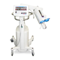
PPI Card
8 - 1
Pre-Programmed Injection -
PPI Card
Bus Buffers The control bus is buffered by U3, and the address bus is buffered by
U1 and U2. The bidirectional data bus is buffered by U4 and U5, with
direction defined by one of the lines on the control bus. These data buff
-
ers are enabled by the decoder. The data bus for the primary memory
chip is controlled by U5; the backup memory chip data bus is controlled
by U4.
Decoder Decoder U6 provides the enable lines for the data bus buffers, the
memory chips, and the RS-232C circuit.
PPI Memory Primary PPI memory is provided by 8K RAM chip U9. Backup PPI
memory is provided by U8. The chips are enabled by signals from the
decoder, while outputs are enabled by lines from the control bus.
Memory Comparator The data buses from the primary and backup memory are continuously
compared by U7. If the values do not agree, latch U11 sends a signal
(MEMERRINT), enabling the CTC on the I/O Card, to interrupt the pro
-
cessor.
Analog Switches The enable lines for the memory chips are switched through U16. When
power is applied, the switches are closed, connecting the enable lines.
When power is removed or low, the switches are open, disabling the
enable lines to preserve power.
Power-Down and
Battery Circuit
When power is removed, or is low, Q1-Q3 disables U16 and opens the
analog switches to disable the memory chips to conserve power as they
switch over to battery power. The battery provides backup power for
the memory chips to preserve the contents when power is removed.
RS-232C Circuit This circuit consists of Universal Asynchronous Receiver/Transmitter
(UART) U13, baud rate clock U12, U19 RS-232 line driver and receiver,
and ferrite beads FB1-FB5 added for reduction of conducted noise.
With this circuit, the main unit can communicate with the Control Panel
using an RS-232C serial interface.
Ferrite Beads FB1-FB5 are used to suppress noise from the power source.
8