3-37
1
2
3
4
2
6
7
8
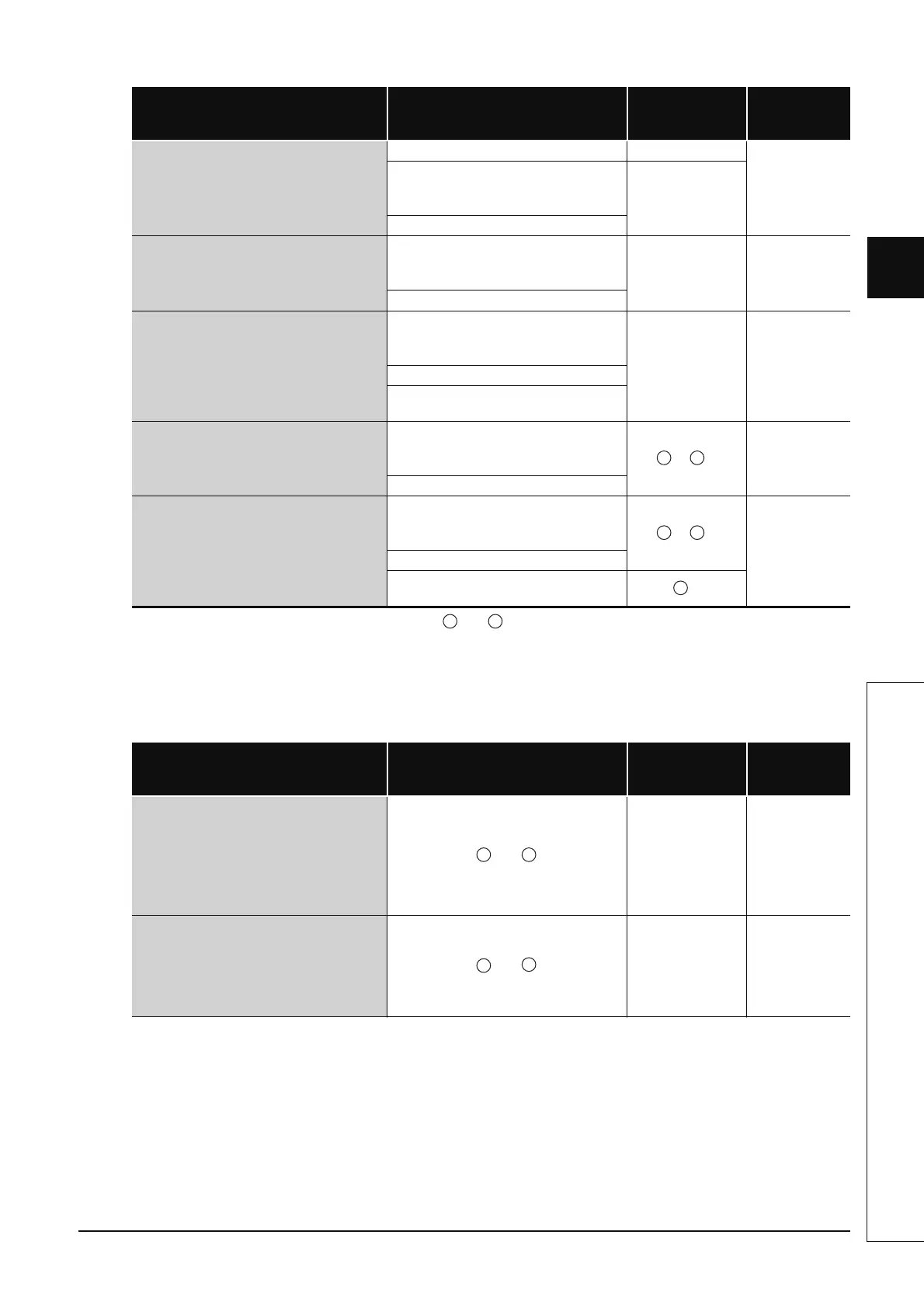
3.8 Counting Step Number
*1: If the same device is used for and , the number of basic steps increases by one.
*2: The number of steps decreases with a standard device register.
When multiple standard device registers are used in an instruction applicable
to subset processing, the number of steps decreases. The following table
shows the number of steps for each instruction.
*3: Not available with LCPU.
Instruction Symbols Devices with Additional Steps
Added Steps
(Number of
Instruction Steps)
Basic Number of
Steps
INC,INCP,DEC,DECP,DINC,DINCP,
DDEC,DDECP
Index register/Standard device register *
2
-1
2
Serial number access format file register
Extended data register (D),
Extended link register (W)
3
Multiple CPU shared device*
3
MOV,MOVP
Serial number access format file register
Extended data register (D),
Extended link register (W)
12
Multiple CPU shared device*
3
DMOV,DMOVP,EMOV,EMOVP
Serial number access format file register
Extended data register (D),
Extended link register (W)
12
Multiple CPU shared device*
3
Decimal constant, hexadecimal
constant, real constant
BCD,BCDP,BIN,BINP,FLT,FLTP,CML,CMLP
Serial number access format file register
Extended data register (D),
Extended link register (W)
:1,:2
2
Multiple CPU shared device*
3
DBCD,DBCDP,DBIN,DBINP,INT,INTP,DINT,
DINTP,DFLT,DFLTP,DCML,DCMLP
Serial number access format file register
Extended data register (D),
Extended link register (W)
:1,:2
2
Multiple CPU shared device*
3
Decimal constant, hexadecimal
constant, real constant
:1
Instruction Symbols
Locations Where Standard Device Regis-
ter Is Used
Added Steps
(Number of
Instruction Steps)
Basic Number of
Steps
LD=,LD<>,LD<,LD<=,LD>,LD>=,
AND=,AND<>,AND<,AND<=,AND>,AND>=,
OR=,OR<>,OR<.OR<=,OR>,OR>=
LDD=,LDD<>,LDD<,LDD<=,LDD>,LDD>=,
ANDD=,ANDD<>,ANDD<,ANDD<=,ANDD>,
AND>=,ORD=,ORD<>,ORD<.ORD<=,
ORD>,ORD>=
and
-2(1) 3
+,-,+P,-P,D+,D-,D+P,D-P,
WAND,WOR,WXOR,WXNR,
DAND,DOR,DXOR,DXNR,
WANDP,WORP,WXORP,WXNRP,
DANDP,DORP,DXORP,DXNRP
(2 devices)
and
-2(1) 3
S1 S2
S1 S2
S1
S1 S2
S1 S2
S1
D
 Loading...