4 - 6 4 - 6
MELSEC-Q
4 I/O COMBINED MODULE
(2) Transistor output specifications (sink type)
Type
Specifications
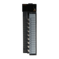
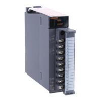
QX41Y41P I/O combined module (output specifications) Appearance
Number of output points 32 points
Isolation method Photocoupler
Rated load voltage 12-24VDC (+20/-15%)
Maximum load current 0.1A/point, 2A/common
Maximum inrush current 0.7A/10ms or less
Leakage current at OFF 0.1mA or lower
Maximum voltage drop at ON 0.1VDC (TYP.) 0.1A, 0.2VDC (MAX.) 0.1A
Response time
OFF ON 1ms or shorter
ON OFF 1ms or shorter (rated load, resistance load)
Surge suppressor Zener diode
Fuse None
External power
supply
Voltage 12-24VDC (+20/-15%) (ripple ratio within 5%)
Current MAX. 15mA /common (when 24VDC and all points are ON)
Common terminal arrangement 32 points/common (common terminal: 2A01, 2A02)
Protection function
Provided (overheat protection function, overload protection function)
• Overheat protection function operate independently of each other.
• Overload protection function operate independently of each other.
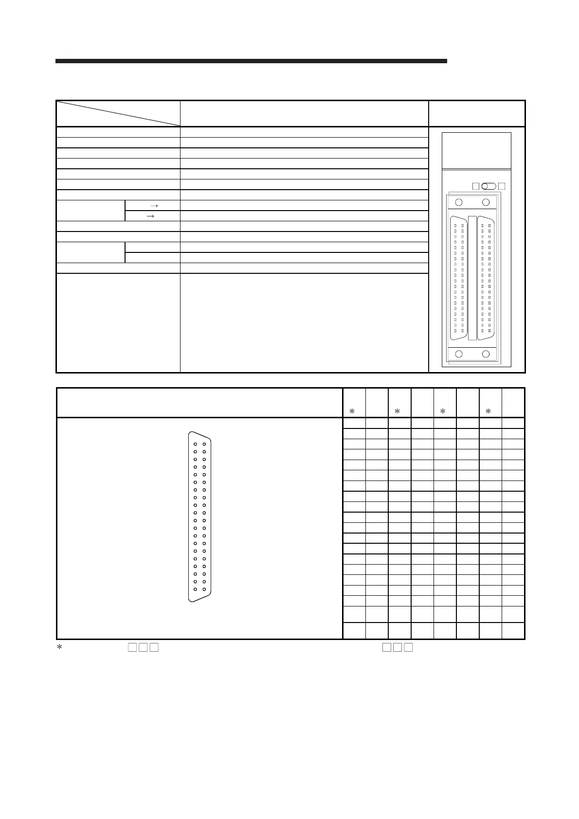
Pin-Outs
Pin
No.
4
Signal
No.
Pin
No.
4
Signal
No.
Pin
No.
4
Signal
No.
Pin
No.
4
Signal
No.
Module front view
1B20 X00 1A20 X10 2B20 Y20 2A20 Y30
1B19 X01 1A19 X11 2B19 Y21 2A19 Y31
1B18 X02 1A18 X12 2B18 Y22 2A18 Y32
1B17 X03 1A17 X13 2B17 Y23 2A17 Y33
1B16 X04 1A16 X14 2B16 Y24 2A16 Y34
1B15 X05 1A15 X15 2B15 Y25 2A15 Y35
1B14 X06 1A14 X16 2B14 Y26 2A14 Y36
1B13 X07 1A13 X17 2B13 Y27 2A13 Y37
1B12 X08 1A12 X18 2B12 Y28 2A12 Y38
1B11 X09 1A11 X19 2B11 Y29 2A11 Y39
1B10 X0A 1A10 X1A 2B10 Y2A 2A10 Y3A
1B09 X0B 1A09 X1B 2B09 Y2B 2A09 Y3B
1B08 X0C 1A08 X1C 2B08 Y2C 2A08 Y3C
1B07 X0D 1A07 X1D 2B07 Y2D 2A07 Y3D
1B06 X0E 1A06 X1E 2B06 Y2E 2A06 Y3E
1B05 X0F 1A05 X1F 2B05 Y2F 2A05 Y3F
1B04 Vacant 1A04 Vacant 2B04 Vacant 2A04 Vacant
1B03 Vacant 1A03 Vacant 2B03 Vacant 2A03 Vacant
1B02 COM1 1A02 Vacant 2B02
12/24
VDC
2A02 COM2
1B01 COM1 1A01 Vacant 2B01
12/24
VDC
2A01 COM2
4: Pin number of 1 indicates that of the left-hand side connector, and pin number of 2 indicates that of the right-hand
side connector.
QX41Y41P
24VDC4mA
12/24VDC
0.1A
QX41Y41P
DISPLAY
F L
01234567
89ABCDEF
01234567
89ABCDEF
A20
A19
A18
A17
A16
A15
A14
A13
A12
A11
A10
A9
A8
A7
A6
A5
A4
A3
A2
A1
B20
B19
B18
B17
B16
B15
B14
B13
B12
B11
B10
B9
B8
B7
B6
B5
B4
B3
B2
B1
 Loading...