Theory of Operation: Main Board 3-9
3.1.2.5 Analog To Digital Converter
The ADC IC's front end down converts the first IF to a second IF, a 2.25 MHz signal, by mixing a
107.4MHz LO signal generated by an integrated synthesizer and external VCO with active device
U602 and resonator L604. The second IF is sampled at 18 MHz, a signal generated by an integrated
clock synthesizer and VCO device with external resonator L605.
The sampled signal is decimated by a factor of 900 to 20 kHz and converted to SSI format at the
ADC's output. The Serial Synchronous Interface (SSI) serial data waveform is composed of a 16 bit
in-phase word (I) followed by a 16 bit Quadrature word (Q). A 20 kHz Frame Synch and a 1.2 MHz
clock waveform are used to synchronize the SSI IQ data transfer to the Digital Signal Processor IC
(OMAP) for post-processing and demodulation.
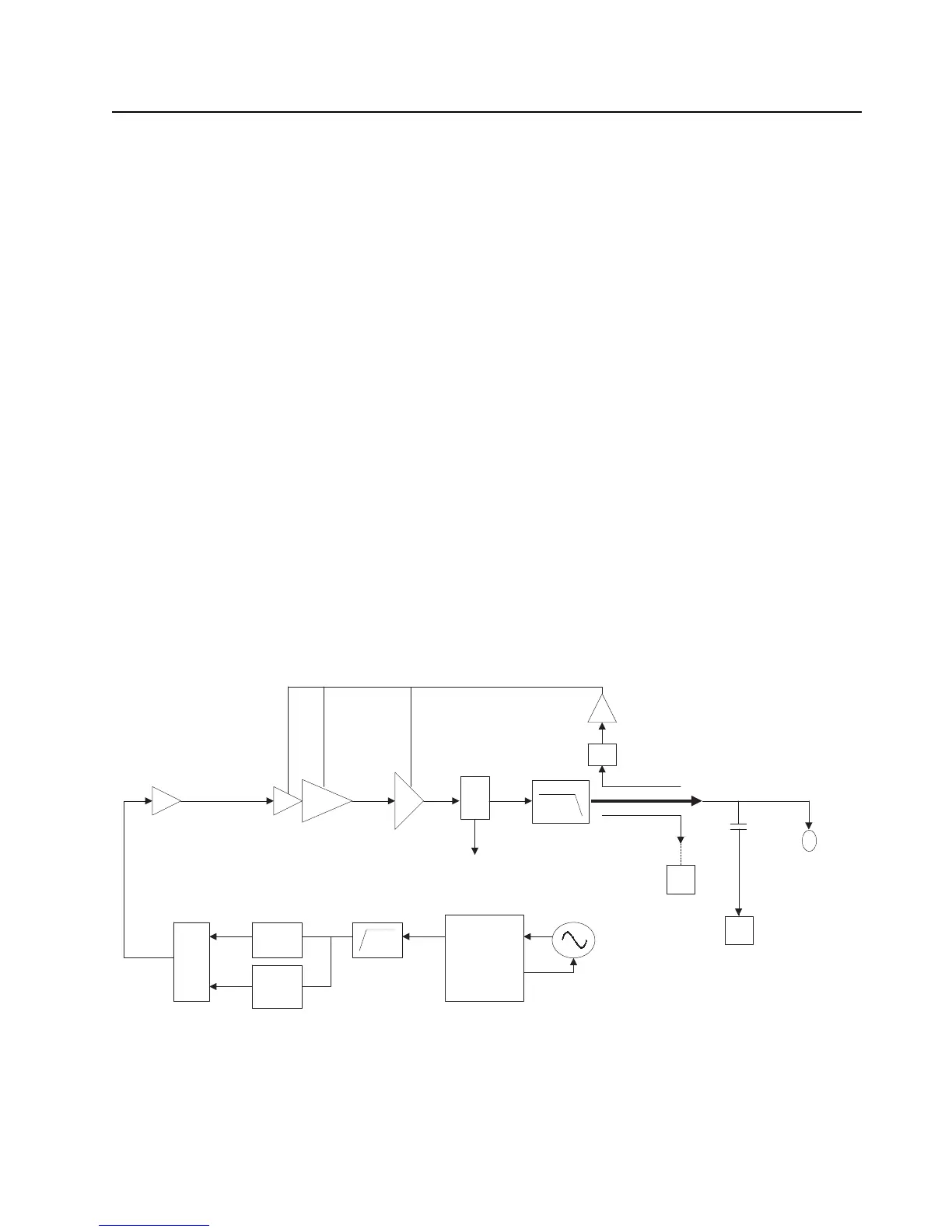
3.1.3 Transmitter
The transmitter takes modulated RF from the FGU and amplifies it to the rated output power to
produce the modulated carrier at the antenna.
NOTE: Refer to List of Transceiver Schematics and Board Overlays for a listing of transmitter-related
schematics that will aid in the following discussion.
The transmitter (Figure 3-9 and Figure 3-10) for the UHF1/UHF2/VHF radio consists of one
MOSFET high power transistor for the UHF1/UHF2/VHF band. The same topology applied for the
700/800 MHz radio (Figure 3-11) where one MOSFET high power transistor is used for the 700/800
MHz band. The high power transistor is driven by an RF driver IC that receives its input signal from
the voltage controlled oscillator. Transmitter power is controlled by a discrete power control circuit
that senses the output of a directional coupler and adjusts PA control voltage to maintain the correct
power level. The TX signals pass through the antenna switch that will provide switching mechanism
from transmit to receive path. The signal then route through each respective harmonic filters, an
embedded directional coupler and finally to the antenna.
Figure 3-9. Transmitter Block Diagram (UHF1/ UHF2)
Trident IC
Synthesizer
Loop Filter
TX VCO
RX
VCO
RF Switch Matrix
TX Buffer Amp
TX Driver Amplifier
Transmitter Final
FET UHF1/UHF2
Harmonic
LP Filter
Ref. Oscillator
Antenna Connecto
Directional
Coupler
Antenna
Switch
TO RX
GPS
Reverse Power
Detection
Log Amp Power Detector
Digital RF Attenuator
 Loading...