Bus Operation
MOTOROLA MC68030 USER’S MANUAL 7-51
State 0
The read cycle starts with S0. The processor drives ECS
low, indicating the beginning of
an external cycle. When the cycle is the first cycle of a read operand operation, OCS
is
driven low at the same time. During S0, the processor places a valid address on A0–A31
and valid function codes on FC0–FC2. The function codes select the address space for
the cycle. The processor drives R/W
high for a read cycle and drives DBEN inactive to
disable the data buffers. SIZ1-SIZ0 become valid, indicating the number of bytes to be
transferred. CIOUT
also becomes valid, indicating the state of the MMU CI bit in the
address translation descriptor or in the appropriate TTx register.
State 1
One-half clock later in S1, the processor asserts AS
, indicating that the address on the
address bus is valid. The processor also asserts DS
during S1. If the burst mode is
enabled for the appropriate on-chip cache and all four long words of the cache entry are
invalid, (i.e., four long words can be read in), CBREQ
is asserted. In addition, the ECS
(and OCS, if asserted) signal is negated during S1.
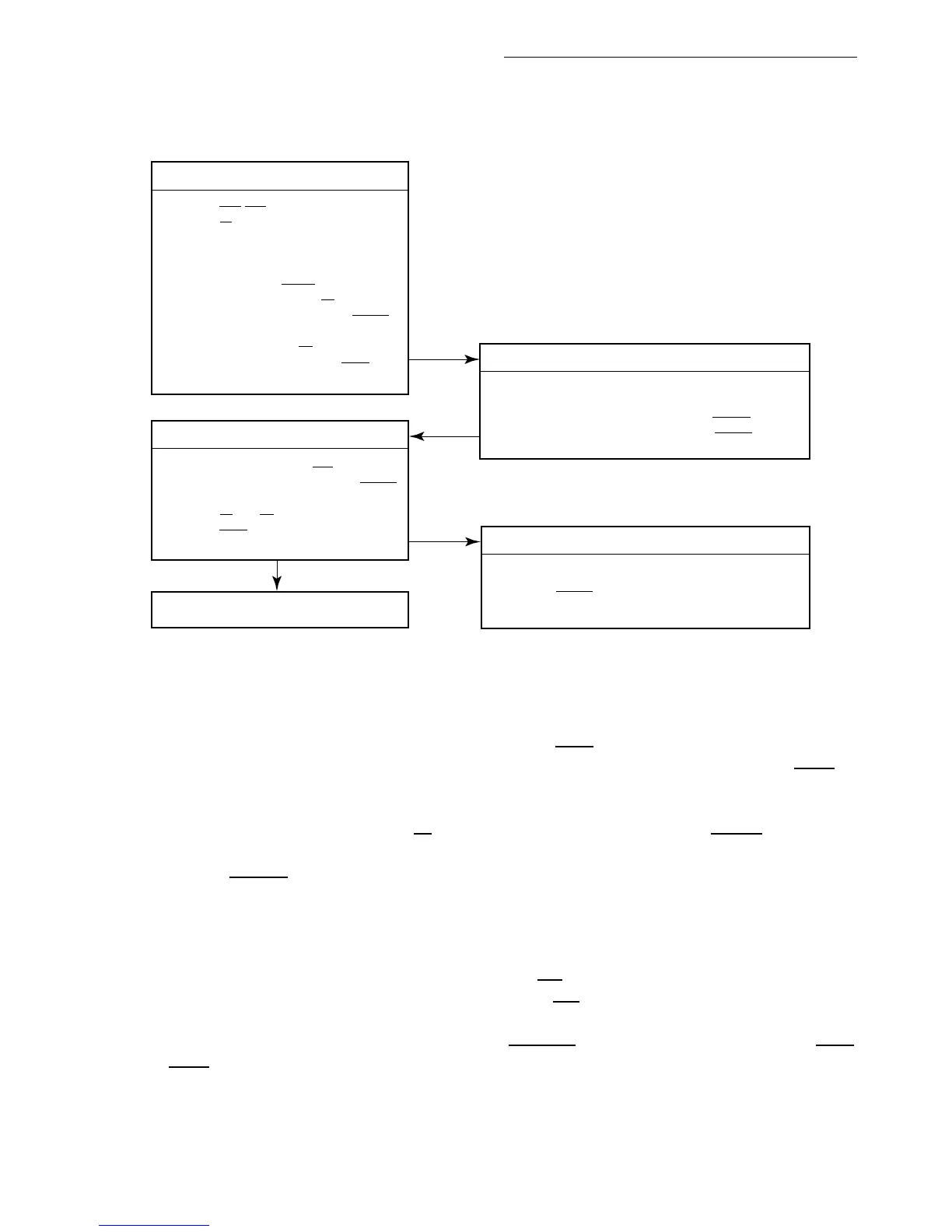
Figure 7-31. Synchronous Long-Word Read Cycle Flowchart —
No Burst Allowed
CONTROLLER
1) ASSERT ECS/OCS FOR ONE-HALF CLOCK
2) DRIVE R/W TO READ
3) DRIVE ADDRESS ON A31–A0
4) DRIVE FUNCTION ON FC2–FC0
5) DRIVE SIZE (SIZ1–SIZ0) (FOUR BYTES)
6) CACHE INHIBIT OUT (CIOUT) BECOMES VALID
7) ASSERT ADDRESS STROBE (AS)
8) ASSERT CACHE BURST REQUEST (CBREQ)
(IF BURST POSSSIBLE)
9) ASSERT DATA STROBE (DS)
10) ASSERT DATA BUFFER ENABLE (DBEN)
1) SAMPLE CACHE INHIBIT IN (CIIN)
AND CACHE BURST ACKNOWLEDGE (CBACK)
2) LATCH DATA
3) NEGATE AS AND DS
4) NEGATE DBEN
PRESENT DATA
1) DECODE ADDRESS
2) PLACE DATA ON D31-D0
3) ASSERT SYNCHRONOUS TERMINATION (STERM)
4) ASSERT CACHE BURST ACKNOWLEDGE (CBACK)
TERMINATE CYCLE
1) REMOVE DATA FROM D31-D0
2) NEGATE STERM
EXTERNAL DEVICE
ADDRESS DEVICE
ACQUIRE DATA
START NEXT CYCLE

 Loading...
