Bus Operation
7-52 MC68030 USER’S MANUAL MOTOROLA
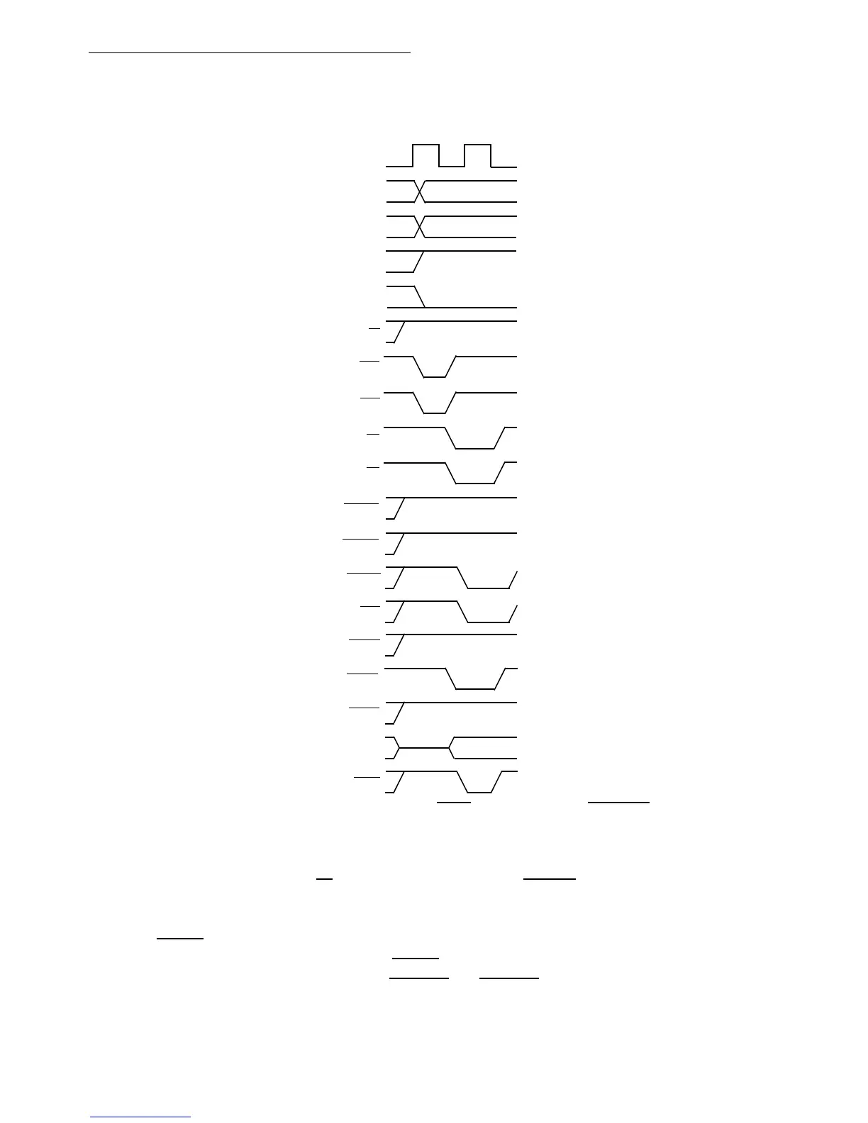
State 2
The selected device uses R/W
, SIZ0–SIZ1, A0–A1, and CIOUT to place its information on
the data bus. Any or all of the byte sections of the data bus (D24–D31, D16–D23, D8–
D15, and D0–D7) are selected by SIZ0–SIZ1 and A0–A1. During S2, the processor
drives DBEN
active to enable external data buffers. In systems that use two-clock
synchronous bus cycles, the timing of DBEN
may prevent its use. At the beginning of S2,
the processor samples the level of STERM
. If STERM is recognized, the processor
latches the incoming data at the end of S2. If the selected data is not to be cached for the
Figure 7-32. Synchronous Read with CIIN
Asserted and CBACK Negated
S0 S2
CLK
A31-A0
D31-D0
ECS
FC2-FC0
SIZ1
SIZ0
R/W
OCS
AS
DS
DSACK1
DSACK0
STERM
CIIN
CIOUT
CBREQ
CBACK
DBEN

 Loading...
