Bus Operation
MOTOROLA MC68030 USER’S MANUAL 7-55
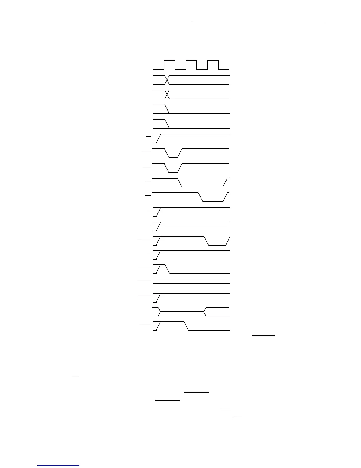
State 2
During S2, the processor places the data to be written onto D0–D31. The selected device
uses R/W
, CLK, SIZ0–SIZ1, and A0–A1 to latch data from the appropriate section(s) of
the data bus (D24–D31, D16–D23, D8–D15, and D0–D7). SIZ0–SIZ1 and A0–A1 select
the data bus sections. The device asserts STERM
when it has successfully stored the
data. If the device does not assert STERM
by the rising edge of S2, the processor inserts
wait states until it is recognized. The processor asserts DS
at the end of S2 if wait states
are inserted. For zero-wait-state synchronous write cycles, DS
is not asserted.
Figure 7-34. Synchronous Write Cycle with Wait States — CIOUT Asserted
CLK
A31-A0
D31-D0
ECS
FC2-FC0
SIZ1
SIZ0
R/W
OCS
AS
DS
DSACK1
DSACK0
STERM
CIIN
CIOUT
CBREQ
CBACK
DBEN
S0 S2 SwS1 Sw S3

 Loading...
