https://reference.digilentinc.com/reference/programmable-logic/nexys-a7/reference-manual 27/30
(https://reference.digilentinc.com/_detail/reference/programmable-logic/nexys-a7/n4ac.png?id=reference%3Aprogrammable-logic%3Anexys-
a7%3Areference-manual) Figure 14.2.1 PDM Timing Diagram
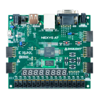
The typical value of the clock frequency is 2.4 MHz (). Assuming that the application requires 7-bit precision and 24 KHz, there can be two
counters that count 128 samples at 12 KHz, as shown in Figure 14.2.2.
(https://reference.digilentinc.com/_detail/reference/programmable-logic/nexys-a7/n4ad.png?id=reference%3Aprogrammable-logic%3Anexys-
a7%3Areference-manual) Figure 14.2.2 Sampling PDM with Two Counters
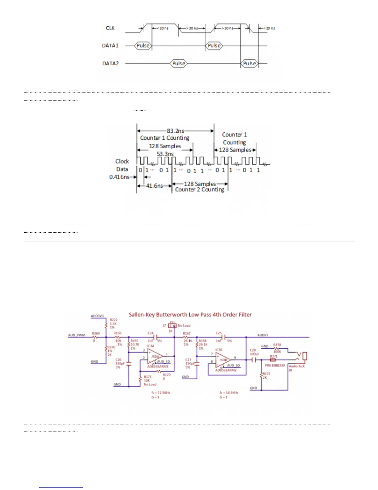
The on-board audio jack (J8) is driven by a Sallen-Key Butterworth Low-pass 4th Order Filter that provides mono audio output. The circuit
of the low-pass filter is shown in Figure 15.1. The input of the filter (AUD_PWM) is connected to the FPGA pin A11. A digital input will
typically be a pulse-width modulated (PWM) or pulse density modulated (PDM) open-drain signal produced by the FPGA. The signal needs
to be driven low for logic ‘0’ and left in high-impedance for logic ‘1’. An on-board pull-up resistor to a clean analog 3.3V rail will establish
the proper voltage for logic ‘1’. The low-pass filter on the input will act as a reconstruction filter to convert the pulse-width modulated
digital signal into an analog voltage on the audio jack output.
(https://reference.digilentinc.com/_detail/reference/programmable-logic/nexys-a7/n4ae.png?id=reference%3Aprogrammable-logic%3Anexys-
a7%3Areference-manual) Figure 15.1 Sallen-Key Butterworth Low-Pass 4th Order Filter
The frequency response of SK Butterworth Low-Pass Filter is shown in Figure 15.2. The AC analysis of the circuit is done using NI
Multisim 12.0.
15 Mono Audio Output