Table 12. Termination of unused pins (continued)
Pin Default state Recommended termination of unused pins
VREFN
—
Tie to VSS
VDDA
—
Tie to VBAT_DCDC
VSSA
—
Tie to VSS
USBn_DP F Can be left unconnected.
USBn_DM F Can be left unconnected.
USBn_3V3 F Tied to VBAT_DCDC.
USB1_VBUS F Tied to VBAT_DCDC.
USBn_VSS F Tied to VSS.
9.3 PCB
For technical reasons, it is best to use a multilayer PCB with a separate layer dedicated to ground (VSS) and another dedicated
to the VDD supply. This provides good decoupling and a good shielding effect. For many applications, economic reasons prohibit
the use of this type of board. In this case, the major requirement is to ensure a good structure for ground and for the power supply.
9.4 General board layout guidelines
9.4.1 Traces recommendations
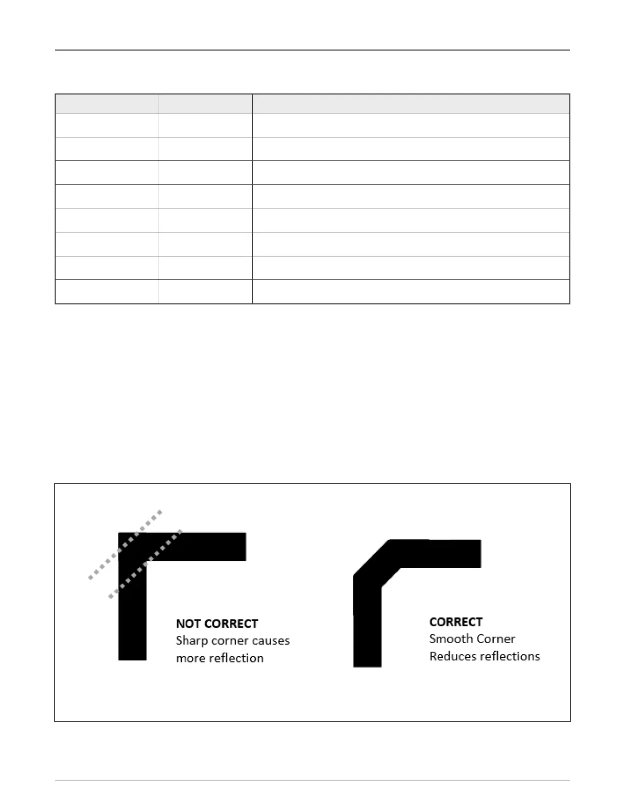
A right angle in a trace can cause more radiation. The capacitance increases in the region of the corner and the characteristic
impedance changes. This impedance change causes reflections. Avoid right-angle bends in a trace and try to route them with at
least two 45° corners. To minimize any impedance change, the best routing would be a round bend, as shown in Figure 12.
Figure 12. Poor and correct way of bending traces in right angles
NXP Semiconductors
Recommendations
Hardware Design Guidelines for LPC55(S)xx Microcontrollers, Rev. 0, 30 October 2020
Application Note 18 / 24
 Loading...


