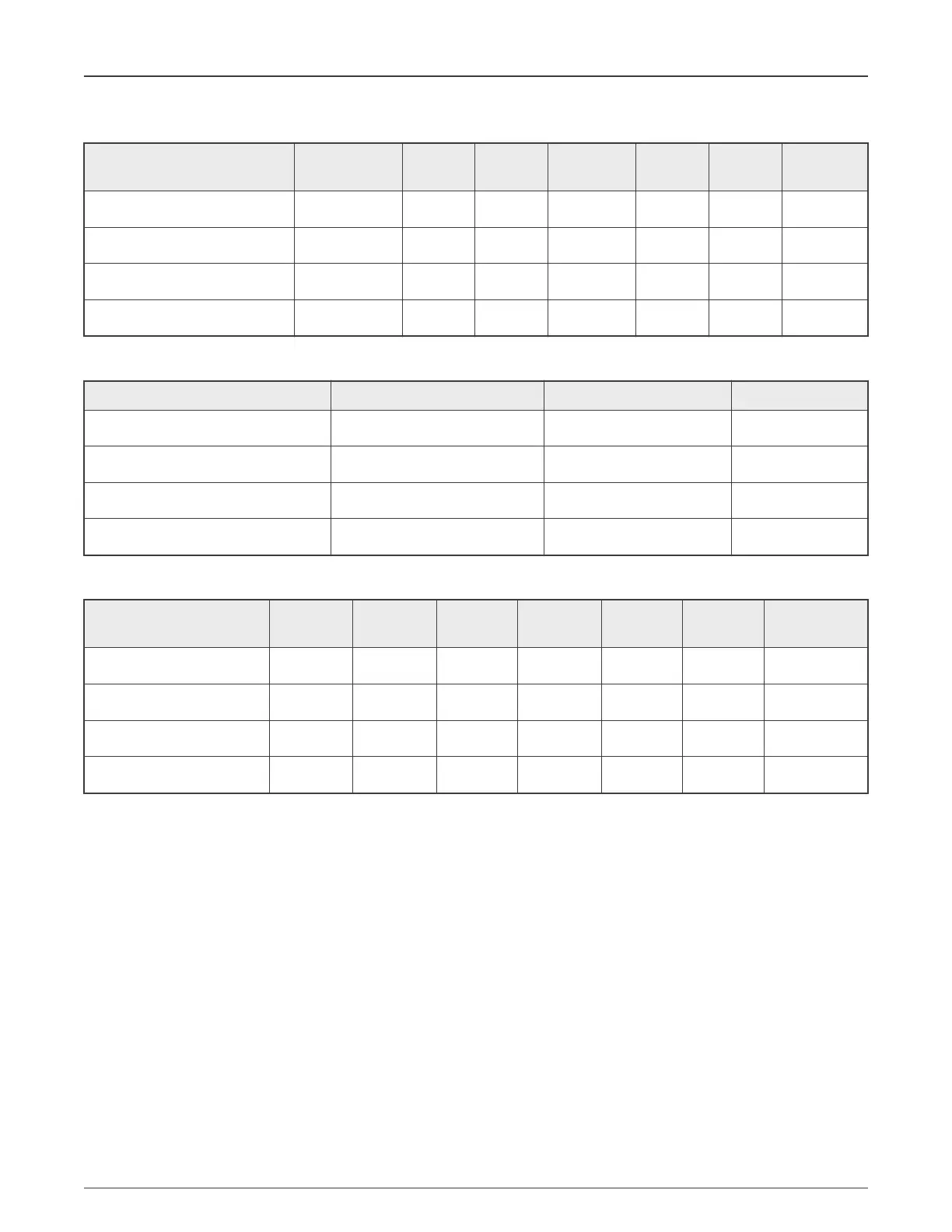
Table 3. LPC55Sxx/LPC55xx Timers
Family CTimer SCT MRT WWDT Code
WDT
RTC OS-Timer
LPC55S0x/LPC550x 5 1 1 1 1 1 1
LPC55S1x/LPC551x 5 1 1 1 1 1 1
LPC55S2x/LPC552x 5 1 1 1
—
1 1
LPC55S6x/LPC556x 5 1 1 1
—
1 1
Table 4. LPC55Sxx/LPC55xx analog peripherals
Family 16 bit ADC Comparator 12 bit DAC
LPC55S0x/LPC550x 1 (10ch)/2 Msps 1 (5 inputs)
—
LPC55S1x/LPC551x 1 (10ch)/2 Msps 1 (5 inputs)
—
LPC55S2x/LPC552x 1 (10ch)/1 Msps 1 (5 inputs)
—
LPC55S6x/LPC556x 1 (10ch)/1 Msps 1 (5 inputs)
—
Table 5. LPC55Sxx/LPC55xx packages
Family HVQFN 48 HVQFN 64 HTQFP 64 VFBGA 98 HLQFP
100
HLQFP
144
VBGA 196
LPC55S0x/LPC550x / /
LPC55S1x/LPC551x / / /
LPC55S2x/LPC552x / / /
LPC55S6x/LPC556x / / /
For details, see the latest version of the Datasheet and User Manuel on www.nxp.com.
3 Power supply
3.1 Introduction
LPC55Sxx series requires single 1.8 to 3.6 V operation voltage supply.
LPC55S0x/LPC550x, LPC55S1x/LPC551x, LPC55S2x/LPC552x and LPC55S6x/LPC556x internal core’s voltage are supplied
by internal DC/DC regulator, this DC/DC regulator needs external inductance and two or three capacitors. For details, see
Using
the DCDC feature
(document AN12325).
NXP Semiconductors
Power supply
Hardware Design Guidelines for LPC55(S)xx Microcontrollers, Rev. 0, 30 October 2020
Application Note 2 / 24
 Loading...


