• Provide adequate filter capacitors on the power supply source. The bulk/bypass and decoupling capacitors should have
low equivalent series inductance (ESL).
• Create ground planes if there are spaces available on the routing layers. Connect these ground areas to the ground plane
with vias.
• Keep the current loops as small as possible. Add as many decoupling capacitors as possible. Always apply current return
rules to reduce loop areas.
• Keep high-speed signals away from other signals and especially away from input and output ports or connectors.
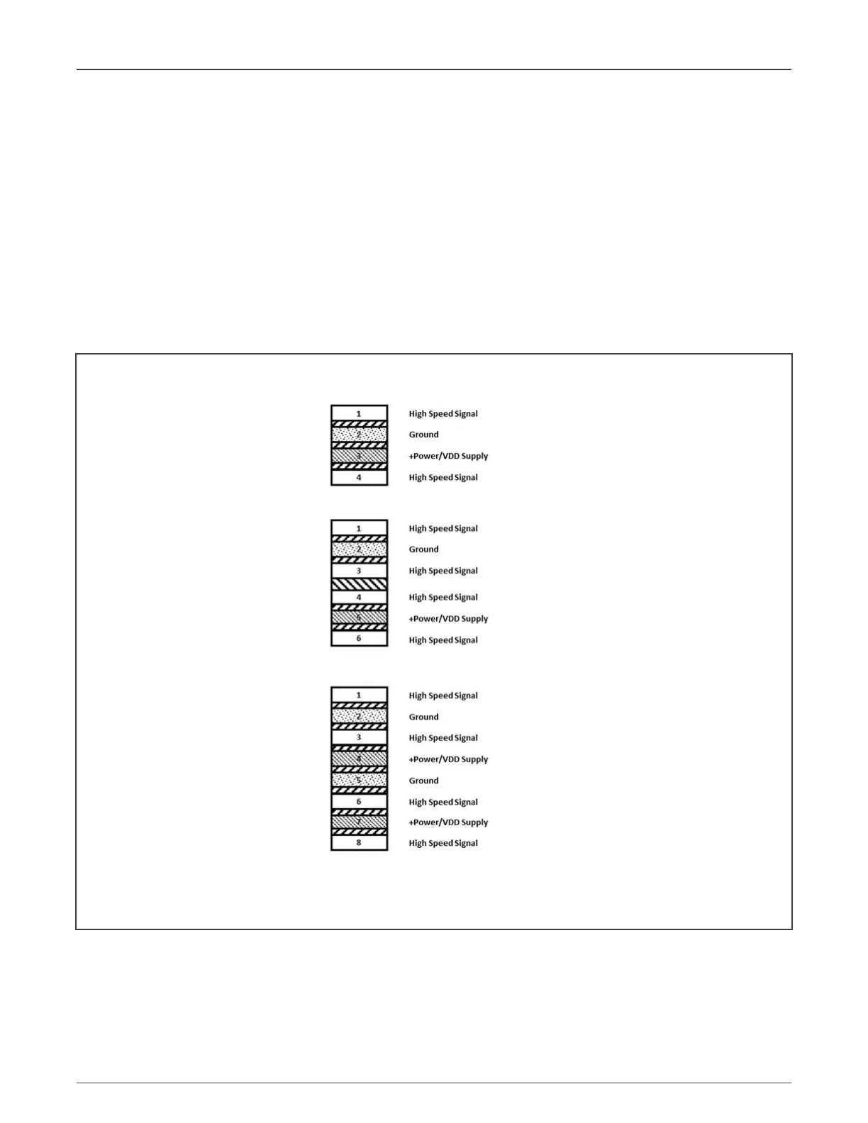
9.4.4 PCB layer stacking
To reach signal integrity and performance requirements, four-layer PCB is recommended for implementing Ethernet applications
and systems. The following layer stack-ups are recommended for four, six, and eight-layer boards, although other options
are possible.
Figure 15. Electromagnetic noise propagation
9.4.5 Injection current
All pins implement protection diodes that protect against Electro Static Discharge (ESD). In many cases, both digital and analog
pins need to be connected to voltages that are higher than the operating voltage of the device pin.
NXP Semiconductors
Recommendations
Hardware Design Guidelines for LPC55(S)xx Microcontrollers, Rev. 0, 30 October 2020
Application Note 22 / 24
 Loading...


